element14 Community
element14 Community
    Register Log In
  • Site
  • Search
  • Log In Register
  • About Us
  • Community Hub
    Community Hub
    • What's New on element14
    • Feedback and Support
    • Benefits of Membership
    • Personal Blogs
    • Members Area
    • Achievement Levels
  • Learn
    Learn
    • Ask an Expert
    • eBooks
    • element14 presents
    • Learning Center
    • Tech Spotlight
    • STEM Academy
    • Webinars, Training and Events
    • Learning Groups
  • Technologies
    Technologies
    • 3D Printing
    • FPGA
    • Industrial Automation
    • Internet of Things
    • Power & Energy
    • Sensors
    • Technology Groups
  • Challenges & Projects
    Challenges & Projects
    • Design Challenges
    • element14 presents Projects
    • Project14
    • Arduino Projects
    • Raspberry Pi Projects
    • Project Groups
  • Products
    Products
    • Arduino
    • Avnet Boards Community
    • Dev Tools
    • Manufacturers
    • Multicomp Pro
    • Product Groups
    • Raspberry Pi
    • RoadTests & Reviews
  • Store
    Store
    • Visit Your Store
    • Choose another store...
      • Europe
      •  Austria (German)
      •  Belgium (Dutch, French)
      •  Bulgaria (Bulgarian)
      •  Czech Republic (Czech)
      •  Denmark (Danish)
      •  Estonia (Estonian)
      •  Finland (Finnish)
      •  France (French)
      •  Germany (German)
      •  Hungary (Hungarian)
      •  Ireland
      •  Israel
      •  Italy (Italian)
      •  Latvia (Latvian)
      •  
      •  Lithuania (Lithuanian)
      •  Netherlands (Dutch)
      •  Norway (Norwegian)
      •  Poland (Polish)
      •  Portugal (Portuguese)
      •  Romania (Romanian)
      •  Russia (Russian)
      •  Slovakia (Slovak)
      •  Slovenia (Slovenian)
      •  Spain (Spanish)
      •  Sweden (Swedish)
      •  Switzerland(German, French)
      •  Turkey (Turkish)
      •  United Kingdom
      • Asia Pacific
      •  Australia
      •  China
      •  Hong Kong
      •  India
      •  Korea (Korean)
      •  Malaysia
      •  New Zealand
      •  Philippines
      •  Singapore
      •  Taiwan
      •  Thailand (Thai)
      • Americas
      •  Brazil (Portuguese)
      •  Canada
      •  Mexico (Spanish)
      •  United States
      Can't find the country/region you're looking for? Visit our export site or find a local distributor.
  • Translate
  • Profile
  • Settings
PCB Design, Prototyping and Production
  • Products
  • More
PCB Design, Prototyping and Production
PCB Forum KiCad 7.0.0 Is Here!
  • Blog
  • Forum
  • Documents
  • Leaderboard
  • Files
  • Members
  • Mentions
  • Sub-Groups
  • Tags
  • More
  • Cancel
  • New
Join PCB Design, Prototyping and Production to participate - click to join for free!
Actions
  • Share
  • More
  • Cancel
Forum Thread Details
  • Replies 29 replies
  • Subscribers 127 subscribers
  • Views 31040 views
  • Users 0 members are here
  • eda
  • kicad
  • schematic capture
  • kicad 7.0
  • ecad
  • pcb
  • pcb design
Related

KiCad 7.0.0 Is Here!

baldengineer
baldengineer over 2 years ago

game gear schematic drawn in KiCad 7

Just slightly over a year since releasing version 6, the development team has released KiCad 7.0!

Something like 1200 (reported) issues were addressed in this update. And an ASIC-load (get it? instead of boat-load...) of new features. You can start the KiCad 7.0 download here. While that chonker downloads, you can read the full announcement or check out my longer KiCad 7 write-up on the release.

My Favorite Two New Features (so far)

Colorizing nets in the Schematic editor was the last thing I played with before the official release. The above image is my version of the Game Gear schematic. (It's in the Bit Preserve GitHub repo.) To help keep the various buses straight, I assigned the bus and its nets to a custom color. I love using this colorization for address, data, and power rails. It really helps things to pop when looking at the schematic.

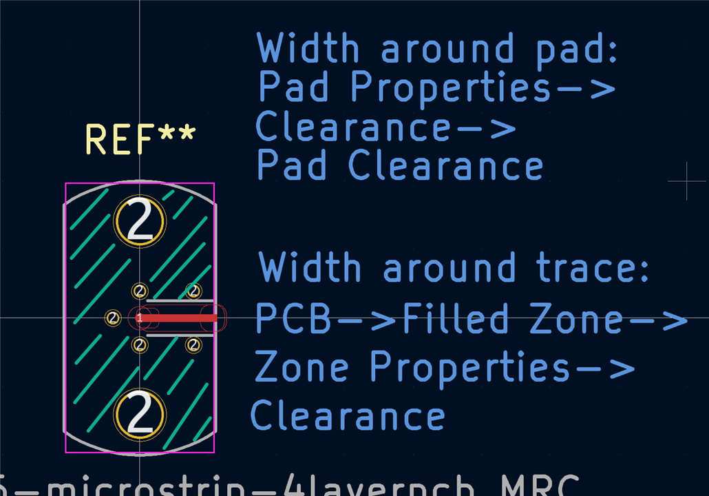
My other favorite feature is the properties panel in PCB. As the name implies, it brings the properties of an element to the top of the UI. First, it saves you from having to "edit" a footprint to adjust its settings. And second, it lets you group multiple similar elements together and change common properties. So, for example, you can grab multiple graphic elements and move them to a different layer without opening any other dialogs!

So, those were the two stand-out features that I really liked. But there are so many more.

Have you used it yet? If so, what do you like (or not like!) about KiCad 7.0?

  • Sign in to reply
  • Cancel

Top Replies

  • Jan Cumps
    Jan Cumps over 2 years ago in reply to baldengineer +4
    who will make the first Comic Sans board?
  • shabaz
    shabaz over 2 years ago +3
    I decided to edit a KiCad 6.0 version board with version 7.0, and happened to use the font capability. The font here looked too informal, so I reverted back to the KiCad standard font after this screenshot…
  • shabaz
    shabaz over 2 years ago +3
    I tried the Pack-and-Move ('P' key) on an older Kicad 6 schematic. It's going to save a HUGE amount of time!
Parents
  • shabaz
    shabaz over 2 years ago

    I've installed it too, (in parallel with existing KiCad 6, with backed-up projects and custom libraries) and it all went well, although I will need to manually locate 3D files for some of the custom library footprints, but I had expected to do that, and it's not a big issue. I'm probably not going to make a PCB with it until a V7 dot-release is available, but I figured it's still a good time to use it to try the new features.

    Several of the new features are super-helpful, especially in the PCB Editor area; the properties pane feature and the 'P' pack-and-move will both save a _lot_ of time.

    The quick line-finish tool (pressing F) in the PCB editor could same some time too. Also, the inverted ('knockout') text is great to see, although it would be nicer if you could draw any filled shape and have the text cut out the filled shape if the text is placed on top. Maybe that's very difficult to implement though, and there are other workarounds anyway.

    The only disappointment for me is that the footprint editor didn't see any properties pane-like functionality at all. It's a pain having to edit each pad one at a time, if a slight tweak needs to be made. Some CAD packages allow for a pad definition to be created separately (I don't like that method, but I can see why they do that). It would be nice to see some sort of solution for rapidly changing all similar pads in one go. Maybe there is a way to do this, but I've not found it yet, and I didn't see anything to indicate that the properties pane will eventually make its way to the footprint editor. 

    My current workaround is to delete all the pads and re-do them all if I need to tweak many pads, but it's not great.

    One other thing that would be nice to see is a way of truncating or splitting lines (e.g. PCB edge cuts, or silkscreen lines) where they intersect. Quite minor, but would be helpful occasionally.

    In summary, using V7 is just as easy as using V6, and from my perspective, it was great to see the new V7 features, particularly in the PCB Editor area,

    • Cancel
    • Vote Up 0 Vote Down
    • Sign in to reply
    • Cancel
  • Jan Cumps
    Jan Cumps over 2 years ago in reply to shabaz
    shabaz said:
    The only disappointment for me is that the footprint editor didn't see any properties pane-like functionality at all.

    ... and no "savvy" fill zone functionality. You can draw areas on the copper layer and fill them. But these areas don't have the same layout-intelligence as a fill zone. What you draw is what you get.

    • Cancel
    • Vote Up +1 Vote Down
    • Sign in to reply
    • Cancel
  • baldengineer
    baldengineer over 2 years ago in reply to Jan Cumps

    I'm not sure I understand what you mean. Do you have an example?

    • Cancel
    • Vote Up +1 Vote Down
    • Sign in to reply
    • Cancel
  • shabaz
    shabaz over 2 years ago in reply to baldengineer

    Hi James.

    I think Jan is referring to scenarios like this, which we came across when trying to create a RF connector footprint. 

    The requirement was to find a way, in the footprint editor, to have copper pour in the green hatched area, which would respect clearance to the thin rectangle red pad. Jan had to manually draw a copper polygon around the red pad, but then if the gap needs to be modified, then it needs to be re-drawn.

    One other workaround is to not put any copper pour in the footprint, and then use a filled zone in the PCB Editor instead. That's what I went with in the end, but it would be nice if the copper pour could have been part of the footprint. 

    It's definitely a niche requirement I guess, but maybe very relevant for RF projects, because there could be other RF parts that could have similar requirements. Maybe we are missing some way of achieving this. I think other PCB packages would struggle too. KiCad is way better than (say) EAGLE, when it comes to complex footprints. With EAGLE it was a case of having to accept so many DRC errors, just to have any semi-complex pads in the footprints. KiCad is a massive improvement.

    However I too am curious if others have come across this requirement too, or how they work around it.

    image

    • Cancel
    • Vote Up 0 Vote Down
    • Sign in to reply
    • Cancel
  • baldengineer
    baldengineer over 2 years ago in reply to shabaz

    Ahhh okay, thanks for the extended explanation. I missed Jan's reference to your comment about the footprint editor.

    (I don't know of a better method than what you've already tried.)

    • Cancel
    • Vote Up 0 Vote Down
    • Sign in to reply
    • Cancel
  • Jan Cumps
    Jan Cumps over 2 years ago in reply to baldengineer

    Indeed, I was referring to the footprint editor

    image

    In the PCB editor, there's (excellent!) support for pour: filled zone

    image

    In the footprint editor, the lower level are your tools to make zones. But they don't have intelligence about anything else on that layer (holes, margins, footprints, thermal relief, ...

    image

    • Cancel
    • Vote Up 0 Vote Down
    • Sign in to reply
    • Cancel
  • baldengineer
    baldengineer over 2 years ago in reply to Jan Cumps

    Sadly, this issue says it was decided not to implement the feature:

    https://gitlab.com/kicad/code/kicad/-/issues/10738

    Specifically this comment: https://gitlab.com/kicad/code/kicad/-/issues/10738#note_865874303

    • Cancel
    • Vote Up +1 Vote Down
    • Sign in to reply
    • Cancel
  • Jan Cumps
    Jan Cumps over 2 years ago in reply to baldengineer

    reusable blocks would be great too Slight smile

    • Cancel
    • Vote Up +2 Vote Down
    • Sign in to reply
    • Cancel
  • shabaz
    shabaz over 2 years ago in reply to baldengineer

    Interesting, good to know it was discussed. I've added a comment on that issue link, to add the RF connector use-case, because it seems that the feature was originally requested for general artwork reasons. I don't know if it is good to add a comment to a closed topic, but I have mentioned I'm happy to create a new request if anyone wants that. 

    • Cancel
    • Vote Up 0 Vote Down
    • Sign in to reply
    • Cancel
  • baldengineer
    baldengineer over 2 years ago in reply to shabaz

    It might be good to open a new issue (and reference that one), but specifically mention RF Connectors.

    At least a couple of years ago, Seth Hildebrand was highly focused on improving KiCad's RF capabilities. He's a lead developer and might have written a plugin in the KiCad 5 era which was intended to prototype features for future versions. (I can't remember if he wrote it, or talked about how the plugin did things he wanted to be native.)

    So I think fresh issues related specifically to RF might get his attention!

    • Cancel
    • Vote Up +1 Vote Down
    • Sign in to reply
    • Cancel
  • shabaz
    shabaz over 2 years ago in reply to baldengineer

    Great! Done, raised here: https://gitlab.com/kicad/code/kicad/-/issues/13934

    • Cancel
    • Vote Up +1 Vote Down
    • Sign in to reply
    • Cancel
  • shabaz
    shabaz over 2 years ago in reply to baldengineer

    There's been an update on this:

    https://gitlab.com/kicad/code/kicad/-/issues/13934

    Jeff there mentions an intriguing method that could work. However, it doesn't seem to work when I tried it, most likely I have done it wrong. But I'll update when there is more info, since the method he mentions could be a good problem-solver.The method uses some trick where a zone could potentially be converted into a polygon, and then one is free to do whatever with that, for instance inserting that polygon into a footprint!

    EDIT: unfortunately that method does not work, but still, it was worth a try!

    • Cancel
    • Vote Up +2 Vote Down
    • Sign in to reply
    • Cancel
Reply
  • shabaz
    shabaz over 2 years ago in reply to baldengineer

    There's been an update on this:

    https://gitlab.com/kicad/code/kicad/-/issues/13934

    Jeff there mentions an intriguing method that could work. However, it doesn't seem to work when I tried it, most likely I have done it wrong. But I'll update when there is more info, since the method he mentions could be a good problem-solver.The method uses some trick where a zone could potentially be converted into a polygon, and then one is free to do whatever with that, for instance inserting that polygon into a footprint!

    EDIT: unfortunately that method does not work, but still, it was worth a try!

    • Cancel
    • Vote Up +2 Vote Down
    • Sign in to reply
    • Cancel
Children
No Data
element14 Community

element14 is the first online community specifically for engineers. Connect with your peers and get expert answers to your questions.

  • Members
  • Learn
  • Technologies
  • Challenges & Projects
  • Products
  • Store
  • About Us
  • Feedback & Support
  • FAQs
  • Terms of Use
  • Privacy Policy
  • Legal and Copyright Notices
  • Sitemap
  • Cookies

An Avnet Company © 2025 Premier Farnell Limited. All Rights Reserved.

Premier Farnell Ltd, registered in England and Wales (no 00876412), registered office: Farnell House, Forge Lane, Leeds LS12 2NE.

ICP 备案号 10220084.

Follow element14

  • X
  • Facebook
  • linkedin
  • YouTube