element14 Community
element14 Community
    Register Log In
  • Site
  • Search
  • Log In Register
  • Community Hub
    Community Hub
    • What's New on element14
    • Feedback and Support
    • Benefits of Membership
    • Personal Blogs
    • Members Area
    • Achievement Levels
  • Learn
    Learn
    • Ask an Expert
    • eBooks
    • element14 presents
    • Learning Center
    • Tech Spotlight
    • STEM Academy
    • Webinars, Training and Events
    • Learning Groups
  • Technologies
    Technologies
    • 3D Printing
    • FPGA
    • Industrial Automation
    • Internet of Things
    • Power & Energy
    • Sensors
    • Technology Groups
  • Challenges & Projects
    Challenges & Projects
    • Design Challenges
    • element14 presents Projects
    • Project14
    • Arduino Projects
    • Raspberry Pi Projects
    • Project Groups
  • Products
    Products
    • Arduino
    • Avnet & Tria Boards Community
    • Dev Tools
    • Manufacturers
    • Multicomp Pro
    • Product Groups
    • Raspberry Pi
    • RoadTests & Reviews
  • About Us
    About the element14 Community
  • Store
    Store
    • Visit Your Store
    • Choose another store...
      • Europe
      •  Austria (German)
      •  Belgium (Dutch, French)
      •  Bulgaria (Bulgarian)
      •  Czech Republic (Czech)
      •  Denmark (Danish)
      •  Estonia (Estonian)
      •  Finland (Finnish)
      •  France (French)
      •  Germany (German)
      •  Hungary (Hungarian)
      •  Ireland
      •  Israel
      •  Italy (Italian)
      •  Latvia (Latvian)
      •  
      •  Lithuania (Lithuanian)
      •  Netherlands (Dutch)
      •  Norway (Norwegian)
      •  Poland (Polish)
      •  Portugal (Portuguese)
      •  Romania (Romanian)
      •  Russia (Russian)
      •  Slovakia (Slovak)
      •  Slovenia (Slovenian)
      •  Spain (Spanish)
      •  Sweden (Swedish)
      •  Switzerland(German, French)
      •  Turkey (Turkish)
      •  United Kingdom
      • Asia Pacific
      •  Australia
      •  China
      •  Hong Kong
      •  India
      •  Japan
      •  Korea (Korean)
      •  Malaysia
      •  New Zealand
      •  Philippines
      •  Singapore
      •  Taiwan
      •  Thailand (Thai)
      •  Vietnam
      • Americas
      •  Brazil (Portuguese)
      •  Canada
      •  Mexico (Spanish)
      •  United States
      Can't find the country/region you're looking for? Visit our export site or find a local distributor.
  • Translate
  • Profile
  • Settings
Raspberry Pi Projects
  • Products
  • Raspberry Pi
  • Raspberry Pi Projects
  • More
  • Cancel
Raspberry Pi Projects
Blog Getting Custom RP2040 Boards Produced and Assembled with KiCad, Part 2!
  • Blog
  • Documents
  • Events
  • Polls
  • Members
  • Mentions
  • Sub-Groups
  • Tags
  • More
  • Cancel
  • New
Join Raspberry Pi Projects to participate - click to join for free!
  • Share
  • More
  • Cancel
Group Actions
  • Group RSS
  • More
  • Cancel
Engagement
  • Author Author: shabaz
  • Date Created: 27 Jun 2026 6:26 PM Date Created
  • Views 327 views
  • Likes 9 likes
  • Comments 10 comments
  • kicad
  • pico
  • PCB production
  • pcb assembly
  • rpiexpert
  • rp2040
  • raspberry_pi_projects
  • production
  • pi pico
Related
Recommended

Getting Custom RP2040 Boards Produced and Assembled with KiCad, Part 2!

shabaz
shabaz
27 Jun 2026

Table of Contents

  • Introduction
  • USB Connector Trace Routing
  • Copper Balancing with Fill Zones
  • 0402 Part Considerations
  • Gerber Time!
  • Speeding Up Creating Your Own Board
  • Preparing for PCB Assembly
  • Summary

Introduction

I wanted to make a custom printed circuit board (PCB) using the RP2040 microcontroller. In Part 1, I covered how I copied the minimal design files from the Raspberry Pi website, made my schematic changes, and then dragged the main bits of the minimal PCB layout onto my desired PCB outline. I now had a PCB containing the minimal design file features (i.e. RP2040, voltage regulator, USB connection and so on) plus my custom add-ons (primarily RS-485 circuitry, but that's unimportant to this blog post).

This blog post covers how I made the project more production-ready. The information here is quite generic, it will apply to non-RP2040 projects too.

image

USB Connector Trace Routing

One minor issue was that the USB connections were in the wrong order for the USB-C connector which I wished to use. I could have mounted the connector on the underside, but that likely would make production more complicated or more expensive. To keep the USB connector on the top side, I had to swap the order by passing one trace through the center of a resistor footprint. It’s not nice, but it shouldn’t matter too much at the 12 MHz rate those traces carry.

image

Note that for board assembly reasons discussed later, you may wish to stick with surface-mount connectors and not through-hole.

Copper Balancing with Fill Zones

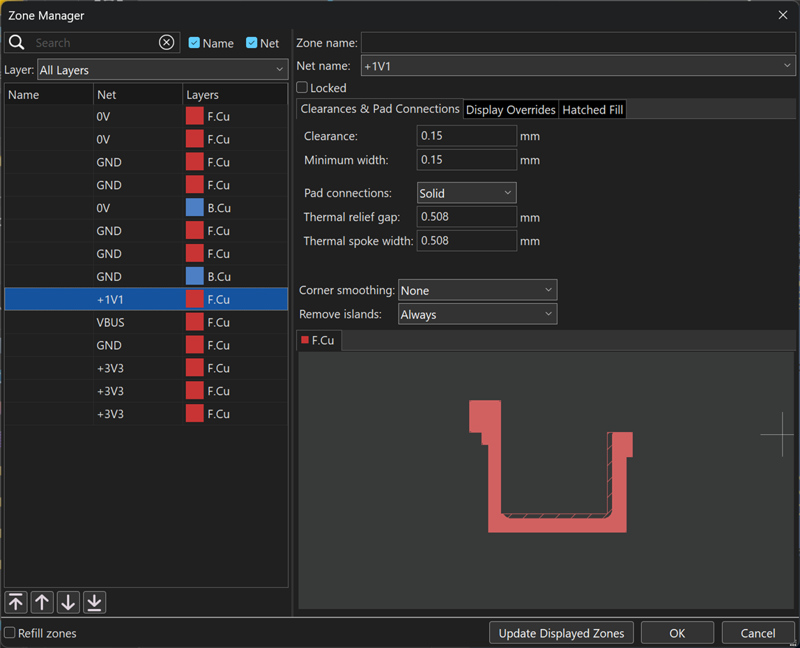
In KiCad, copper can be added to a design by drawing shapes called filled zones. This is important because otherwise PCBs can warp due to unbalanced copper. As copper is added, it is inevitable that eventually a few issues may occur. One is that filled zones may overlap, and you’ll want to control which ones will take priority. KiCad has an excellent Zone Manager tool where you can see a list of all the zones in the design, plus a rendering of what they look like. It’s possible to adjust the zone priorities by moving items up and down the list.
image

Another problem can be that the board layout can be so compact, or component footprint pads so close to one another, that the fill zone might make only minimal contact with the pads that it ought to make contact with, and a design rule check warning will be raised. KiCad design rules by default expect there to be at least two connections between pads and the fill zone, but the RP2040 is very fine pitched (0.4 mm) and two connections are not possible for a few power pins (specifically pins 10, 33, and 49 on the QFN56 package). There are a few ways to get rid of the warning, I decided to edit the footprint in the library, and set those specific pins to ‘None’ for the zone connection strategy, so that I could draw a trace myself in the schematic, to connect those pins to the fill zone. The screenshot below shows those connections.

image

0402 Part Considerations

0402-sized parts are so small, that it’s very likely that the components will slide around or rotate, or even lift off a pad (known as tombstoning) when the solder paste melts during the solder reflow phase of production.

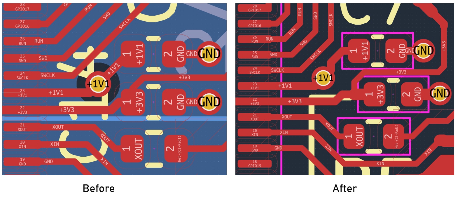
I had to modify the original minimal design, to get traces to attach to pads in a more centered and end-on fashion, and avoid traces coming off at angles. See the before and after screenshots.
image

Another thing worth checking, is that are 0402 parts actually necessary? Such tiny parts make production reliability unnecessarily poorer. If you don’t care about the size of a circuit board, and if there’s no electrical reason to have the part so small, then 0603 is a lot more attactive. Personally I would prefer 0603, but for now I kept the components at 0402 size.

Yet another problem can be that CAD packages might have oversized pads for capacitors and resistors. EAGLE CAD software was famous for having huge footprints, KiCad is better, but nevertheless it is worth comparing with actual 0402 component dimensions from datasheets, since the pads ought to be a size very close to the part size, there’s little room for error with such small components.

Gerber Time!

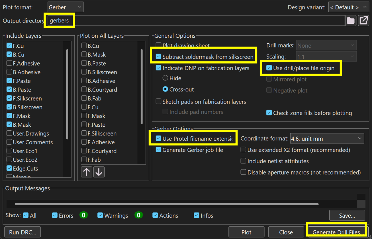
With the PCB layout complete, and the PCB Design Rules Check (DRC) executed, it was time to plot (i.e. generate) the Gerber and drill files, and then inspect the output using the KiCad Gerber Viewer tool.

I found it quite important to ensure Use drill/place file origin was checked, otherwise it created an offset that affected the placement of components in the Preparing for PCB Assembly section further below.
image

Here’s a closeup of the top layer of the final PCB (blue is solder paste, since this board will be reflowed).

I made the silkscreen text a bit larger, because there was space for it. I also added a pinout diagram for the connector I was using for my project, using the Image Converter application supplied with KiCad.

image

image

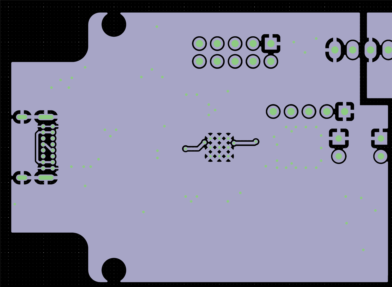
This is the bottom copper; there are a couple of traces in the center that carry the 1.1V core power for the RP2040.

Here’s the final render:

image

Speeding Up Creating Your Own Board

If anyone is interested in trying this themselves using KiCad, I placed my modification of the original minimal design in a custom RP2040 minimal design repository on GitHub.
It will save quite a bit of time use these files, compared to working with the original minimal design files. However, please note the board is untested currently, since I still need to get it produced.

This is the circuit diagram of the design I placed on GitHub:

image

PCB render:

image

Hopefully that's a good start to adding your custom circuitry.

Preparing for PCB Assembly

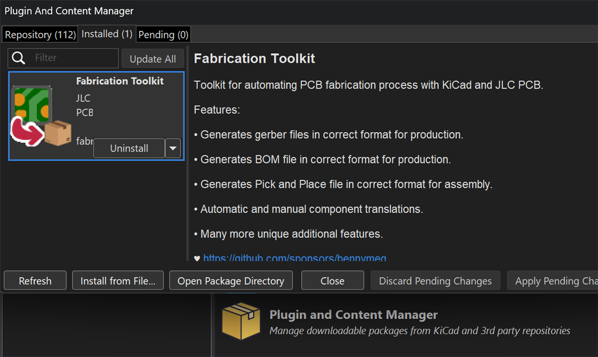
Now that the PCB layout is complete, I will need to supply some files (CSV format) that explain to the manufacturer what components need to be populated and where. I installed a KiCad plugin called Fabrication Toolkit to help create those files.
image

I also need to decide, do I purchase the components and send them to the board manufacturer/assembly firm, or do I request them to provide the parts?

With KiCad schematics, it is possible to use Tools->Bulk Edit Symbol Fields to add distributor part codes fields, that the fabrication toolkit can read to generate the required output.

image

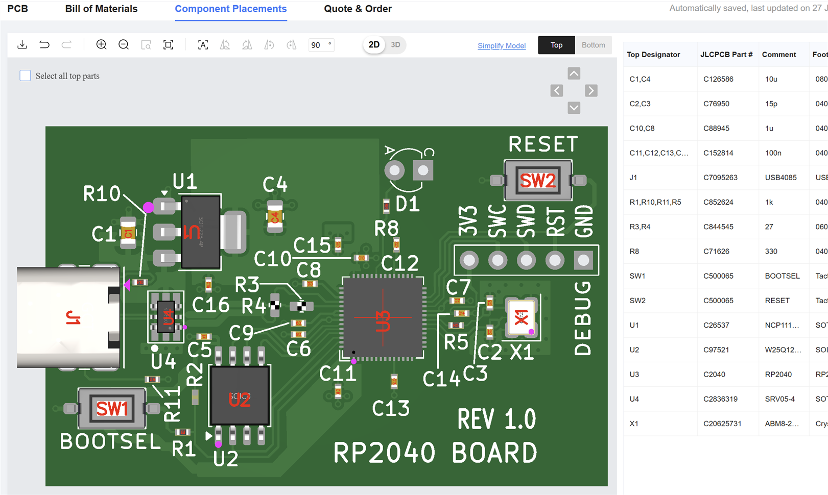
With the PCB manufacturer that I’m planning to use, adding the PCB assembly service is quite easy; I uploaded the Gerber files as usual for a PCB-only order, then scrolled down and clicked on PCB Assembly which was listed at the bottom. Then, I clicked Next and the website requested me to upload a couple of the files (BOM and Position CSV files) that were generated by the Fabrication Toolkit. The website then listed all the parts for review, then I clicked Next to see a PCB assembly render:
image

The purple dots indicates what the manufacturer thinks is pin 1. You’ll notice U4 is wrongly oriented, and R3 and R4 were unknown to the manufacturer. The simplest fix for R3 and R4 will be to choose different resistors (I just got unlucky selecting the ones that I did), and click on U4 and click on an icon just above the board rendering, to rotate. Personally I will try to fix in KiCad, and then re-upload, rather than make changes on the PCB assembly website.

I clicked Next again, and the cost was listed. This is for a quantity of 10, not including shipping and tax. You can see that I would have saved about $7 if I’d used a surface-mount USB-C connector instead of the one I did.

image

Summary

There are quite a few details to consider when trying to produce complete PCB assemblies, and it is easy to miss things. I am not a PCB assembly manufacturing expert (and don’t wish to be, to be honest!), and have no doubt missed a load of things.

I have only touched on a few topics; in reality, one would create a checklist and run through it all, to ensure that the board is ready for production, whereas I skipped all that, considered a few basics (copper fill to avoid board warping and I tried to make the layout less likely to cause 0402 assembly issues), and I only briefly visually inspected the PCB Gerber files. In reality, to reduce self-stress and improve board production success chances, it is worthwhile finding a friend/colleague and sharing out the tasks, using each other to review the design and everything on your checklist. 

It’s important to review the schematic, component selection, footprints, and PCB layout. Furthermore, it would be good to just get a few boards assembled, and test them, before committing to larger quantities.

Click here for the concluding Part 3 blog.

Thanks for reading!

  • Sign in to reply

Top Comments

  • shabaz
    shabaz 14 days ago +1
    I've updated the PCB at the RP2040 custom minimal board repository , so that is uses a surface-mount connector suggested by geralds and it's simplified the USB data lines routing too. I tried uploading…
  • geralds
    geralds 9 days ago in reply to shabaz

    Hi  shabaz 

    Wow! Thank you so much! I've read your GitHub repository. Great!

    KiCad keeps crashing:

    In my opinion, the problem might be partly due to Windows 11, specifically the combination of hard drive type (nowadays it's flash storage).

    This operating system has a lot of background processes running, so programs often freeze briefly.

    I'm also using Windows 11 Pro.

    KiCad seems "kind of cobbled together," that's my impression.

    I'm monitoring this now because it can't be that I have a modern, up-to-date system that's malfunctioning somewhere.

    I frequently check the Event Viewer in the system settings.

    • Cancel
    • Vote Up 0 Vote Down
    • Sign in to reply
    • More
    • Cancel
  • shabaz
    shabaz 9 days ago in reply to geralds

    Hi Gerald,

    This is great! I have added it to the GitHub repo. Thank you for this! 

    Regarding KiCad crashing with DRC checks, sadly this is quite common, I don't know the reason, but every version of KiCad I have ever used (6 through 10, I use the Windows version, not tried Linux) has done that. I am just used to saving before running DRC (even without saving, usually KiCad is good with recovery and also has automated backups, so I've never actually lost any work (maybe a few minutes of work very rarely). But it's really bizarre how every KiCad version tends to crash with DRC.

    • Cancel
    • Vote Up 0 Vote Down
    • Sign in to reply
    • More
    • Cancel
  • geralds
    geralds 10 days ago in reply to shabaz

    Hi  shabaz 

    Awesome!

    I've just finished my version.

    So, starting with your Rev2, I made my Rev3 with the new USB connector and changes to the PCB, including component relocations and trace optimizations.
    I also adjusted the USB traces, hopefully optimizing them, and surrounded them with a ground shield.
    I also repositioned the voltage regulator, rotating it to accommodate the USB connector.
    I placed the passive components on the 603 footprints, and the capacitors according to their capacitances.
    I optimized the clock's placement.

    image  image 

    image  image

    The project folder with all files. Hopefully that is right for your project.

    RP2040_minimal-edit_V3.zip

    Schematic:

    Sorry.... I'm not a KiCad user, normally I work with Fusion360, so, since last few weeks I learned a lot about KiCad.

    And, yes, this KiCad project was very easy importing into Fusion, there were some wrongs, but they are not fatal.  

    And phew...: I had to adjust the components because there was a mistake in their design.
    The USB receptacle had a line on the "Edge Cuts" layer of the footprint, right under the component outline.
    The DRC check kept throwing errors until I discovered this fine, short, hidden line.

    The KiCad's library also contains the footprint for the RP2040, which had also been created incorrectly. It has fatal errors (DRC).
    There was a polygon on the BOT layer.
    Finding this error in the DRC check was a nightmare, ugh...
    Therefore, I also modified this footprint and added several pin holes to it, Pin 57.

    And, last but not least, the KiCad PCB app kept crashing mostly during the DRC check and after saving in between; also, the schematics editor crashed sometimes if I wanted to edit some properties of the symbols.

    Furthermore, I wanted the entire project in one project folder on the D drive, where there are many different projects in electronics, mechanics, and physics.
    That was an ordeal! I wasted several hours trying to consolidate the project databases into one project folder.

    KiCad has databases in the C:..user folder, in the C:..program folder (where the complete KiCad database is), and when you create new components, they are saved everywhere, including in the project folder.

    And you have to pay close attention to where each part is stored in order to copy it over.

    Wow, I managed to combine all the components.

    Well then, this board is now finished.

    No errors in the DRC check!

    If you'd like, and if it works for you, you can incorporate my impressions into your version and save it to Git.

    That's where I found your files, too.

    Best regards,
    Gerald
    ---

    • Cancel
    • Vote Up 0 Vote Down
    • Sign in to reply
    • More
    • Cancel
  • shabaz
    shabaz 11 days ago in reply to shabaz

    That was super fast. It's done!

    image

    image

    • Cancel
    • Vote Up 0 Vote Down
    • Sign in to reply
    • More
    • Cancel
  • shabaz
    shabaz 12 days ago in reply to shabaz

    It is too late for me to do anything (I've already placed the order), but I just noticed that the few through-hole parts (which were going to be manual-assembled) are not actually manually-soldered, they will be wave soldered. Unfortunately, that raises two issues: (1) I didn't make any considerations for that, and I'm not aware of the direction of the wave, so I couldn't orient parts in any particular way (or orient through-hole pad shapes) and (2) I have unpopulated header pin holes, they may end up plugged with solder : ( I don't know if they will cover those areas up beforehand.

    Both of these issues are repairable if they occur of course. Maybe the best solution for small volume is to avoid through-hole assembly, and do that after the boards arrive if needed.

    • Cancel
    • Vote Up 0 Vote Down
    • Sign in to reply
    • More
    • Cancel
>
element14 Community

element14 is the first online community specifically for engineers. Connect with your peers and get expert answers to your questions.

  • Members
  • Learn
  • Technologies
  • Challenges & Projects
  • Products
  • Store
  • About Us
  • Feedback & Support
  • FAQs
  • Terms of Use
  • Privacy Policy
  • Legal and Copyright Notices
  • Sitemap
  • Cookies

An Avnet Company © 2026 Premier Farnell Limited. All Rights Reserved.

Premier Farnell Ltd, registered in England and Wales (no 00876412), registered office: Farnell House, Forge Lane, Leeds LS12 2NE.

Follow element14

  • X
  • Facebook
  • linkedin
  • YouTube