element14 Community
element14 Community
    Register Log In
  • Site
  • Search
  • Log In Register
  • Community Hub
    Community Hub
    • What's New on element14
    • Feedback and Support
    • Benefits of Membership
    • Personal Blogs
    • Members Area
    • Achievement Levels
  • Learn
    Learn
    • Ask an Expert
    • eBooks
    • element14 presents
    • Learning Center
    • Tech Spotlight
    • STEM Academy
    • Webinars, Training and Events
    • Learning Groups
  • Technologies
    Technologies
    • 3D Printing
    • FPGA
    • Industrial Automation
    • Internet of Things
    • Power & Energy
    • Sensors
    • Technology Groups
  • Challenges & Projects
    Challenges & Projects
    • Design Challenges
    • element14 presents Projects
    • Project14
    • Arduino Projects
    • Raspberry Pi Projects
    • Project Groups
  • Products
    Products
    • Arduino
    • Avnet & Tria Boards Community
    • Dev Tools
    • Manufacturers
    • Multicomp Pro
    • Product Groups
    • Raspberry Pi
    • RoadTests & Reviews
  • About Us
    About the element14 Community
  • Store
    Store
    • Visit Your Store
    • Choose another store...
      • Europe
      •  Austria (German)
      •  Belgium (Dutch, French)
      •  Bulgaria (Bulgarian)
      •  Czech Republic (Czech)
      •  Denmark (Danish)
      •  Estonia (Estonian)
      •  Finland (Finnish)
      •  France (French)
      •  Germany (German)
      •  Hungary (Hungarian)
      •  Ireland
      •  Israel
      •  Italy (Italian)
      •  Latvia (Latvian)
      •  
      •  Lithuania (Lithuanian)
      •  Netherlands (Dutch)
      •  Norway (Norwegian)
      •  Poland (Polish)
      •  Portugal (Portuguese)
      •  Romania (Romanian)
      •  Russia (Russian)
      •  Slovakia (Slovak)
      •  Slovenia (Slovenian)
      •  Spain (Spanish)
      •  Sweden (Swedish)
      •  Switzerland(German, French)
      •  Turkey (Turkish)
      •  United Kingdom
      • Asia Pacific
      •  Australia
      •  China
      •  Hong Kong
      •  India
      •  Japan
      •  Korea (Korean)
      •  Malaysia
      •  New Zealand
      •  Philippines
      •  Singapore
      •  Taiwan
      •  Thailand (Thai)
      •  Vietnam
      • Americas
      •  Brazil (Portuguese)
      •  Canada
      •  Mexico (Spanish)
      •  United States
      Can't find the country/region you're looking for? Visit our export site or find a local distributor.
  • Translate
  • Profile
  • Settings
Raspberry Pi Projects
  • Products
  • Raspberry Pi
  • Raspberry Pi Projects
  • More
  • Cancel
Raspberry Pi Projects
Blog Getting Custom RP2040 Boards Produced and Assembled with KiCad, Part 2!
  • Blog
  • Documents
  • Events
  • Polls
  • Members
  • Mentions
  • Sub-Groups
  • Tags
  • More
  • Cancel
  • New
Join Raspberry Pi Projects to participate - click to join for free!
  • Share
  • More
  • Cancel
Group Actions
  • Group RSS
  • More
  • Cancel
Engagement
  • Author Author: shabaz
  • Date Created: 27 Jun 2026 6:26 PM Date Created
  • Views 638 views
  • Likes 9 likes
  • Comments 10 comments
  • kicad
  • pico
  • PCB production
  • pcb assembly
  • rpiexpert
  • rp2040
  • raspberry_pi_projects
  • production
  • pi pico
Related
Recommended

Getting Custom RP2040 Boards Produced and Assembled with KiCad, Part 2!

shabaz
shabaz
27 Jun 2026

Table of Contents

  • Introduction
  • USB Connector Trace Routing
  • Copper Balancing with Fill Zones
  • 0402 Part Considerations
  • Gerber Time!
  • Speeding Up Creating Your Own Board
  • Preparing for PCB Assembly
  • Summary

Introduction

I wanted to make a custom printed circuit board (PCB) using the RP2040 microcontroller. In Part 1, I covered how I copied the minimal design files from the Raspberry Pi website, made my schematic changes, and then dragged the main bits of the minimal PCB layout onto my desired PCB outline. I now had a PCB containing the minimal design file features (i.e. RP2040, voltage regulator, USB connection and so on) plus my custom add-ons (primarily RS-485 circuitry, but that's unimportant to this blog post).

This blog post covers how I made the project more production-ready. The information here is quite generic, it will apply to non-RP2040 projects too.

image

USB Connector Trace Routing

One minor issue was that the USB connections were in the wrong order for the USB-C connector which I wished to use. I could have mounted the connector on the underside, but that likely would make production more complicated or more expensive. To keep the USB connector on the top side, I had to swap the order by passing one trace through the center of a resistor footprint. It’s not nice, but it shouldn’t matter too much at the 12 MHz rate those traces carry.

image

Note that for board assembly reasons discussed later, you may wish to stick with surface-mount connectors and not through-hole.

Copper Balancing with Fill Zones

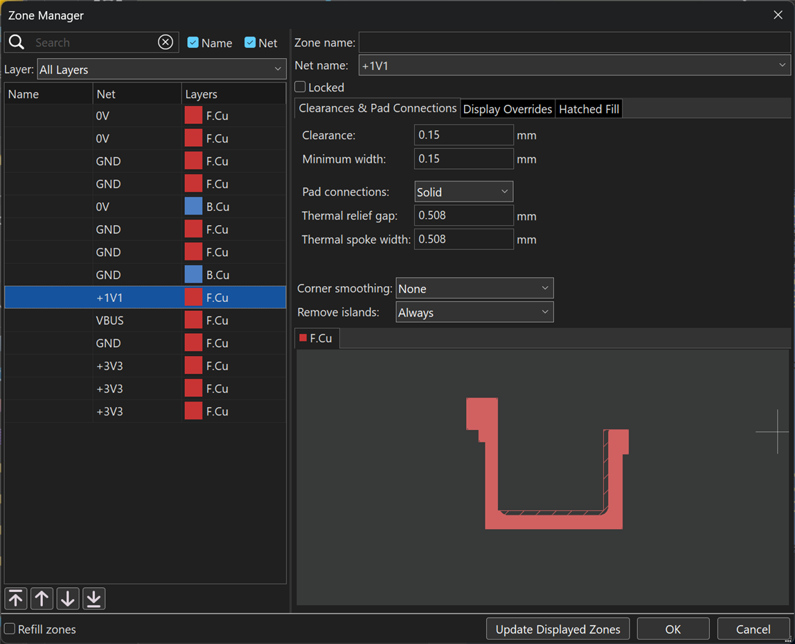
In KiCad, copper can be added to a design by drawing shapes called filled zones. This is important because otherwise PCBs can warp due to unbalanced copper. As copper is added, it is inevitable that eventually a few issues may occur. One is that filled zones may overlap, and you’ll want to control which ones will take priority. KiCad has an excellent Zone Manager tool where you can see a list of all the zones in the design, plus a rendering of what they look like. It’s possible to adjust the zone priorities by moving items up and down the list.
image

Another problem can be that the board layout can be so compact, or component footprint pads so close to one another, that the fill zone might make only minimal contact with the pads that it ought to make contact with, and a design rule check warning will be raised. KiCad design rules by default expect there to be at least two connections between pads and the fill zone, but the RP2040 is very fine pitched (0.4 mm) and two connections are not possible for a few power pins (specifically pins 10, 33, and 49 on the QFN56 package). There are a few ways to get rid of the warning, I decided to edit the footprint in the library, and set those specific pins to ‘None’ for the zone connection strategy, so that I could draw a trace myself in the schematic, to connect those pins to the fill zone. The screenshot below shows those connections.

image

0402 Part Considerations

0402-sized parts are so small, that it’s very likely that the components will slide around or rotate, or even lift off a pad (known as tombstoning) when the solder paste melts during the solder reflow phase of production.

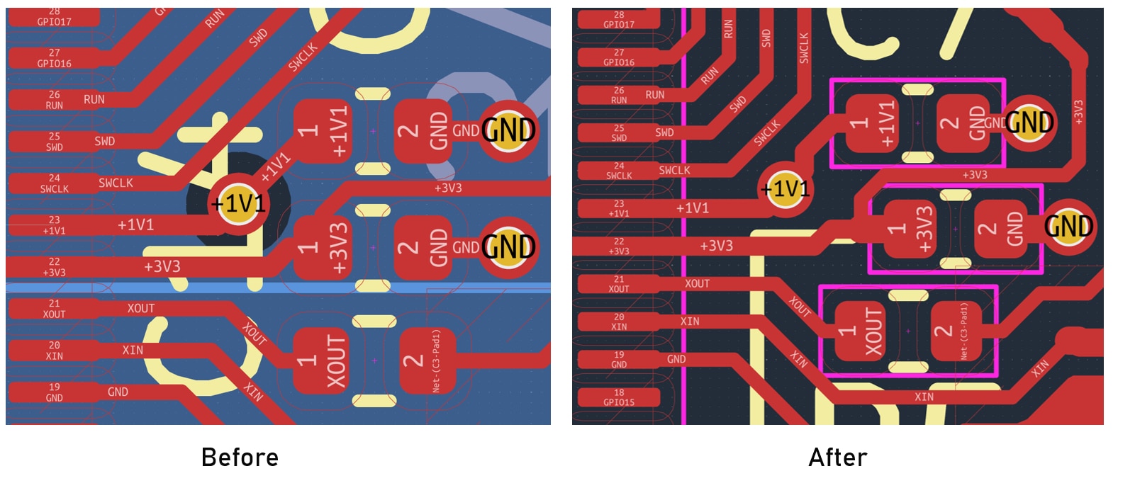
I had to modify the original minimal design, to get traces to attach to pads in a more centered and end-on fashion, and avoid traces coming off at angles. See the before and after screenshots.
image

Another thing worth checking, is that are 0402 parts actually necessary? Such tiny parts make production reliability unnecessarily poorer. If you don’t care about the size of a circuit board, and if there’s no electrical reason to have the part so small, then 0603 is a lot more attactive. Personally I would prefer 0603, but for now I kept the components at 0402 size.

Yet another problem can be that CAD packages might have oversized pads for capacitors and resistors. EAGLE CAD software was famous for having huge footprints, KiCad is better, but nevertheless it is worth comparing with actual 0402 component dimensions from datasheets, since the pads ought to be a size very close to the part size, there’s little room for error with such small components.

Gerber Time!

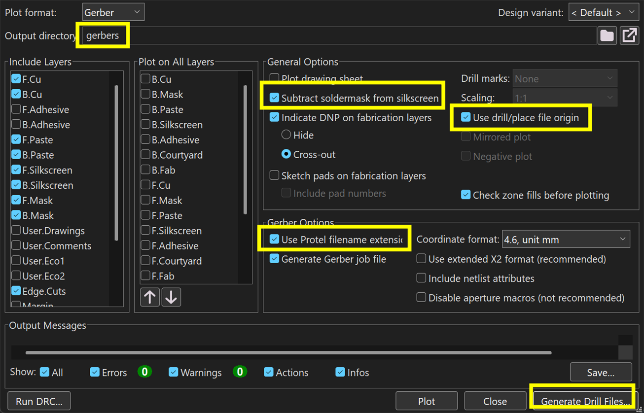
With the PCB layout complete, and the PCB Design Rules Check (DRC) executed, it was time to plot (i.e. generate) the Gerber and drill files, and then inspect the output using the KiCad Gerber Viewer tool.

I found it quite important to ensure Use drill/place file origin was checked, otherwise it created an offset that affected the placement of components in the Preparing for PCB Assembly section further below.
image

Here’s a closeup of the top layer of the final PCB (blue is solder paste, since this board will be reflowed).

I made the silkscreen text a bit larger, because there was space for it. I also added a pinout diagram for the connector I was using for my project, using the Image Converter application supplied with KiCad.

image

image

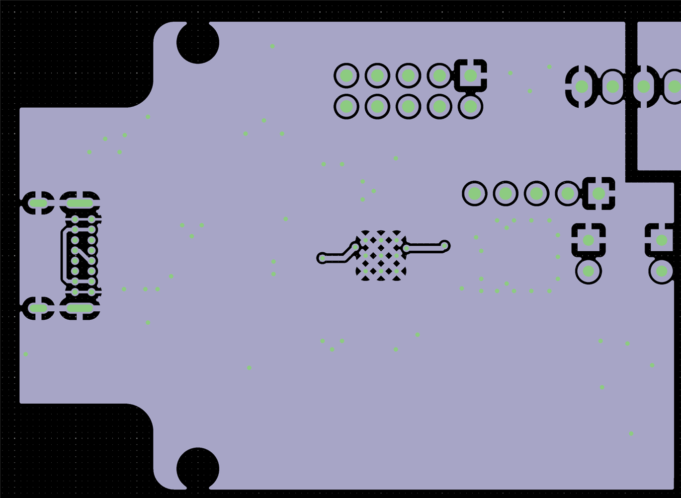
This is the bottom copper; there are a couple of traces in the center that carry the 1.1V core power for the RP2040.

Here’s the final render:

image

Speeding Up Creating Your Own Board

If anyone is interested in trying this themselves using KiCad, I placed my modification of the original minimal design in a custom RP2040 minimal design repository on GitHub.
It will save quite a bit of time use these files, compared to working with the original minimal design files. However, please note the board is untested currently, since I still need to get it produced.

This is the circuit diagram of the design I placed on GitHub:

image

PCB render:

image

Hopefully that's a good start to adding your custom circuitry.

Preparing for PCB Assembly

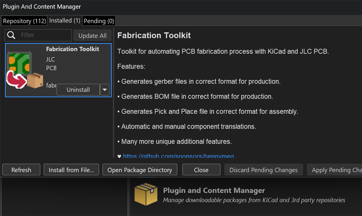
Now that the PCB layout is complete, I will need to supply some files (CSV format) that explain to the manufacturer what components need to be populated and where. I installed a KiCad plugin called Fabrication Toolkit to help create those files.
image

I also need to decide, do I purchase the components and send them to the board manufacturer/assembly firm, or do I request them to provide the parts?

With KiCad schematics, it is possible to use Tools->Bulk Edit Symbol Fields to add distributor part codes fields, that the fabrication toolkit can read to generate the required output.

image

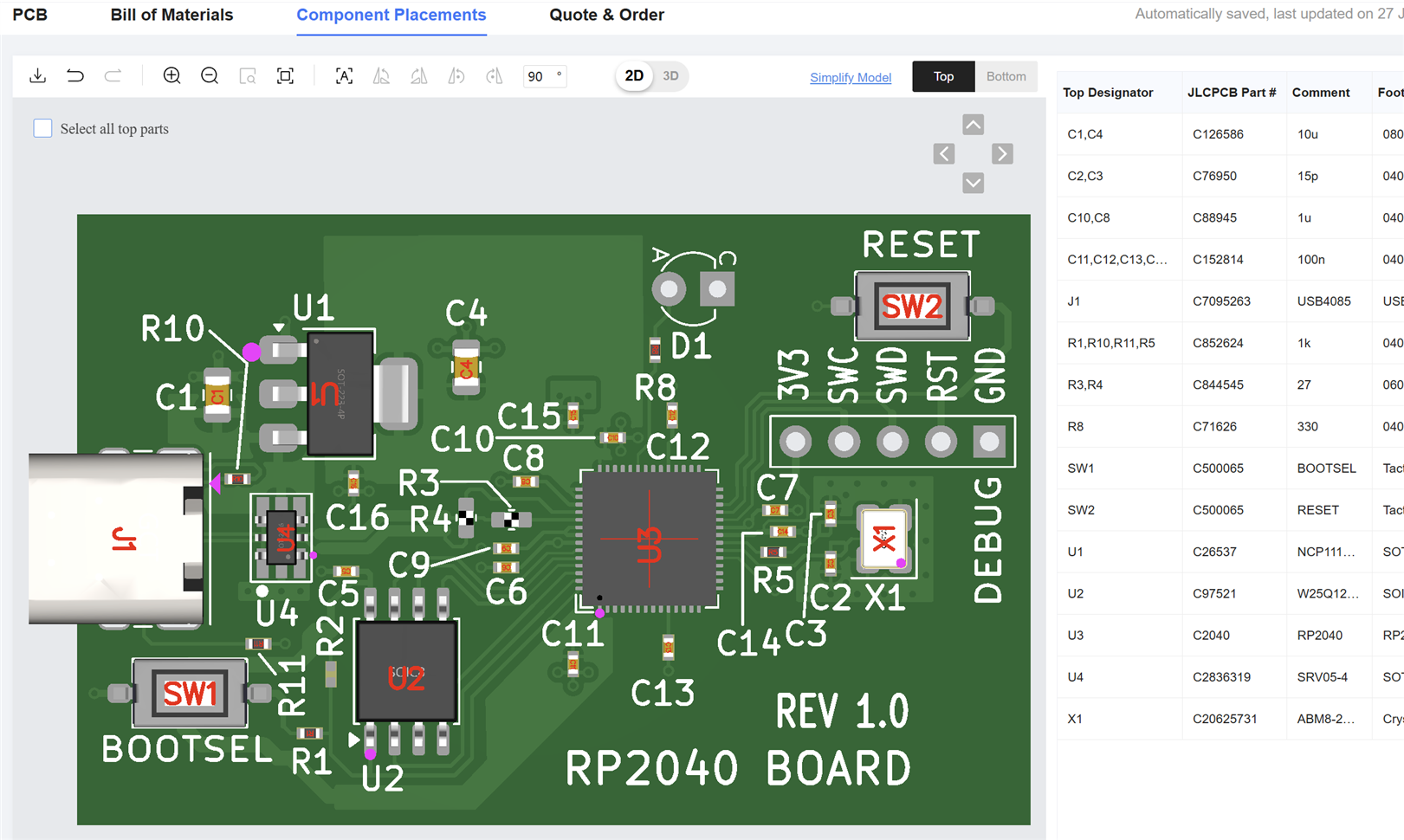
With the PCB manufacturer that I’m planning to use, adding the PCB assembly service is quite easy; I uploaded the Gerber files as usual for a PCB-only order, then scrolled down and clicked on PCB Assembly which was listed at the bottom. Then, I clicked Next and the website requested me to upload a couple of the files (BOM and Position CSV files) that were generated by the Fabrication Toolkit. The website then listed all the parts for review, then I clicked Next to see a PCB assembly render:
image

The purple dots indicates what the manufacturer thinks is pin 1. You’ll notice U4 is wrongly oriented, and R3 and R4 were unknown to the manufacturer. The simplest fix for R3 and R4 will be to choose different resistors (I just got unlucky selecting the ones that I did), and click on U4 and click on an icon just above the board rendering, to rotate. Personally I will try to fix in KiCad, and then re-upload, rather than make changes on the PCB assembly website.

I clicked Next again, and the cost was listed. This is for a quantity of 10, not including shipping and tax. You can see that I would have saved about $7 if I’d used a surface-mount USB-C connector instead of the one I did.

image

Summary

There are quite a few details to consider when trying to produce complete PCB assemblies, and it is easy to miss things. I am not a PCB assembly manufacturing expert (and don’t wish to be, to be honest!), and have no doubt missed a load of things.

I have only touched on a few topics; in reality, one would create a checklist and run through it all, to ensure that the board is ready for production, whereas I skipped all that, considered a few basics (copper fill to avoid board warping and I tried to make the layout less likely to cause 0402 assembly issues), and I only briefly visually inspected the PCB Gerber files. In reality, to reduce self-stress and improve board production success chances, it is worthwhile finding a friend/colleague and sharing out the tasks, using each other to review the design and everything on your checklist. 

It’s important to review the schematic, component selection, footprints, and PCB layout. Furthermore, it would be good to just get a few boards assembled, and test them, before committing to larger quantities.

Click here for the concluding Part 3 blog.

Thanks for reading!

  • Sign in to reply

Top Comments

  • shabaz
    shabaz 1 month ago +1
    I've updated the PCB at the RP2040 custom minimal board repository , so that is uses a surface-mount connector suggested by geralds and it's simplified the USB data lines routing too. I tried uploading…
  • shabaz
    shabaz 1 month ago

    I gave it a try! This is the minimal board with the additions I wanted. I uploaded the PCB files, and then at the bottom of the website clicked on PCB Assembly.

    The website prompted me for the BoM and Component Positions files (which were auto-generated by KiCad by clicking on the icon that got installed with the Fabrication Toolkit plugin).

    Then, I had to visually go over this rendering that the site created, to check all component positions and orientations were correct. 

    image

    This was the costing for a quantity of 10 (which is excessive, really I should only try a few boards first, but worst case I'll manually do some rework on these boards if needed).

    image

    With tax and DHL shipping all included, it worked out to $214 total, which is £169, i.e. £16.90 per board.

    • Cancel
    • Vote Up 0 Vote Down
    • Sign in to reply
    • More
    • Cancel
  • shabaz
    shabaz 1 month ago

    I've updated the PCB at the RP2040 custom minimal board repository, so that is uses a surface-mount connector suggested by geralds and it's simplified the USB data lines routing too.

    I tried uploading the design to a usual PCB manufacturer, and it looks good. 

    image

    Here's the costing for ten boards (add your shipping costs and tax on top of that).

    image

    Of course, this is just for informational purposes, I'm not going to order this specific board as-is, since it's a minimal design with no GPIO connected (apart from an LED!). It is up to the user to append their own circuitry, e.g. header pins if nothing else).

    A couple of points regarding the online assembly service experience so far:

    (1) It can happen that the PCB assembly manufacturer is unable to render some of the components in the 3D view. They were displayed with a checkerbox pattern. I believe that means the manufacturer will ckeck the layout manually, so instead I decided to change the component to one that was recognized. This was an annoying iterative process admittedly.

    (2) Some components can appear with an offset or incorrect rotation. Rotations can be solved immediately by clicking an icon in the 3D view on the website (this is the simplest way but like me, some might prefer to go back and modify in their files), but if there is an offset, that's more long-winded. I had to move the component in the footprint editor (i.e. select all, then right-click and from the pop-up menu in KiCad go to Position->Move Exactly), which is really annoying since of course that means that the PCB needs to be modified because the component will move. For example, the USB connector was off the PCB by precisely 5 mm (I don't know why!). My original (0,0) position, i.e. origin of the component, was at the location shown with the red arrow. That position made sense to me, because it was the most important reference mechanically, it is where the connector ends. However, I had to move the component such that the origin was at the green arrow location, 5 mm inward. In practise, while this is feasible with the very simple board that I had, with a more complex board you definitely won't want to be doing this. You could edit the positions in the CSV file generated by the Fabrication Toolkit in KiCad, but then you'd need to remember to re-edit that, if you ever re-ran that toolkit. Probably best to make a checklist and add notes for such things for the specific board, so you don't forget.

    image

    One other observation, is that all this might seem like a lot of work to set up, and it really is. But then when I thought about it, manufacturing an entire board should rightly be expected to be a lot of work. Normally that's a whole team-worth of work (design engineers, PCB engineers, mechanical engineers, parts procurement and parts library management, and so on), so it's impressive a lot of that can be collapsed into an online ordering process, but you do still need to do an amount of work to get through it.

    • Cancel
    • Vote Up +1 Vote Down
    • Sign in to reply
    • More
    • Cancel
  • geralds
    geralds 1 month ago in reply to shabaz

    Hi Shabaz,

    I just read your second part; I'll read it again more carefully because there are some details there that also apply to my board. Yes, I'll also change the resistors and capacitors to 603s.

    The USB was important to me so you'd have a full connection option, since the library only contains standard components.

    Well, the SMD version would also be good, but for this application, as you say, this "oops" solution at 12 MHz is sufficient.

    The paired routing of the data lines in KiCad needs to be modified further (to 90 ohms), I think. // That's just my initial impression regarding the impedance; unfortunately, the cheap solution with the crossing using the two vias on the D- line is the way to go.

    I specifically avoided sending data under the second resistor, as that creates interference in the other (D+) line. That's why I went with the more open solution using the vias.

    Even at the USB port, where the A and B connections cross, I see I've placed the D- line on the lower layer.

    I actually wanted to place the D+ line on the lower layer. Please place the D+ line on the lower layer. This will roughly balance them out.

    The respective line lengths aren't a perfect match, but at this slow speed, it's sufficient to avoid data dispersion.

    Tip: I often compare this to the data cabling that runs across an office. RF applications on the board are similar ---> NEXT, FEXT, SKEW (differences in line length create signal skewness and dispersion, which you then see in the transfer monitor, jitter, etc.)

    • Cancel
    • Vote Up 0 Vote Down
    • Sign in to reply
    • More
    • Cancel
  • shabaz
    shabaz 1 month ago in reply to geralds

    Hi Gerald,

    Thanks! I've decided to use the USB trace via method as you describe, it's simpler than messing about with the way I used. I'm also going to look at some point for a SMD alternative for the USB-C connector I normally use. Even if it costs more, it may work out lower-cost with assembly, plus, there's one less production step to cause potential issues.

    • Cancel
    • Vote Up 0 Vote Down
    • Sign in to reply
    • More
    • Cancel
  • geralds
    geralds 1 month ago

    Hi  shabaz 

    Wow! superb! They are very fine information's that I can use.

    Please look I've answered and uploaded my Ki-Cad files in part 1.

    image

    image

    Best Regards Gerald

    • Cancel
    • Vote Up 0 Vote Down
    • Sign in to reply
    • More
    • Cancel
<
element14 Community

element14 is the first online community specifically for engineers. Connect with your peers and get expert answers to your questions.

  • Members
  • Learn
  • Technologies
  • Challenges & Projects
  • Products
  • Store
  • About Us
  • Feedback & Support
  • FAQs
  • Terms of Use
  • Privacy Policy
  • Legal and Copyright Notices
  • Sitemap
  • Cookies

An Avnet Company © 2026 Premier Farnell Limited. All Rights Reserved.

Premier Farnell Ltd, registered in England and Wales (no 00876412), registered office: Farnell House, Forge Lane, Leeds LS12 2NE.

Follow element14

  • X
  • Facebook
  • linkedin
  • YouTube