element14 Community
element14 Community
    Register Log In
  • Site
  • Search
  • Log In Register
  • Community Hub
    Community Hub
    • What's New on element14
    • Feedback and Support
    • Benefits of Membership
    • Personal Blogs
    • Members Area
    • Achievement Levels
  • Learn
    Learn
    • Ask an Expert
    • eBooks
    • element14 presents
    • Learning Center
    • Tech Spotlight
    • STEM Academy
    • Webinars, Training and Events
    • Learning Groups
  • Technologies
    Technologies
    • 3D Printing
    • FPGA
    • Industrial Automation
    • Internet of Things
    • Power & Energy
    • Sensors
    • Technology Groups
  • Challenges & Projects
    Challenges & Projects
    • Design Challenges
    • element14 presents Projects
    • Project14
    • Arduino Projects
    • Raspberry Pi Projects
    • Project Groups
  • Products
    Products
    • Arduino
    • Avnet & Tria Boards Community
    • Dev Tools
    • Manufacturers
    • Multicomp Pro
    • Product Groups
    • Raspberry Pi
    • RoadTests & Reviews
  • About Us
    About the element14 Community
  • Store
    Store
    • Visit Your Store
    • Choose another store...
      • Europe
      •  Austria (German)
      •  Belgium (Dutch, French)
      •  Bulgaria (Bulgarian)
      •  Czech Republic (Czech)
      •  Denmark (Danish)
      •  Estonia (Estonian)
      •  Finland (Finnish)
      •  France (French)
      •  Germany (German)
      •  Hungary (Hungarian)
      •  Ireland
      •  Israel
      •  Italy (Italian)
      •  Latvia (Latvian)
      •  
      •  Lithuania (Lithuanian)
      •  Netherlands (Dutch)
      •  Norway (Norwegian)
      •  Poland (Polish)
      •  Portugal (Portuguese)
      •  Romania (Romanian)
      •  Russia (Russian)
      •  Slovakia (Slovak)
      •  Slovenia (Slovenian)
      •  Spain (Spanish)
      •  Sweden (Swedish)
      •  Switzerland(German, French)
      •  Turkey (Turkish)
      •  United Kingdom
      • Asia Pacific
      •  Australia
      •  China
      •  Hong Kong
      •  India
      •  Japan
      •  Korea (Korean)
      •  Malaysia
      •  New Zealand
      •  Philippines
      •  Singapore
      •  Taiwan
      •  Thailand (Thai)
      •  Vietnam
      • Americas
      •  Brazil (Portuguese)
      •  Canada
      •  Mexico (Spanish)
      •  United States
      Can't find the country/region you're looking for? Visit our export site or find a local distributor.
  • Translate
  • Profile
  • Settings
Raspberry Pi Projects
  • Products
  • Raspberry Pi
  • Raspberry Pi Projects
  • More
  • Cancel
Raspberry Pi Projects
Blog Making a Custom RP2040 Project with KiCad, Part 1!
  • Blog
  • Documents
  • Events
  • Polls
  • Members
  • Mentions
  • Sub-Groups
  • Tags
  • More
  • Cancel
  • New
Join Raspberry Pi Projects to participate - click to join for free!
  • Share
  • More
  • Cancel
Group Actions
  • Group RSS
  • More
  • Cancel
Engagement
  • Author Author: shabaz
  • Date Created: 24 Jun 2026 3:25 PM Date Created
  • Views 1277 views
  • Likes 9 likes
  • Comments 32 comments
  • kicad
  • pico
  • rpiexpert
  • rp2040
  • raspberry_pi_projects
  • pi pico
Related
Recommended

Making a Custom RP2040 Project with KiCad, Part 1!

shabaz
shabaz
24 Jun 2026

Partly out of curiosity, and partly to test some aspects of a workflow for other projects, I decided to create a custom RP2040 board. In most cases, there’s no need to do this; it may well be more expensive than simply using a ready-made Raspberry Pi Pico module and mounting it on a custom PCB, while saving a considerable amount of effort.

This short blog post describes how I’m approaching the project. It’s very much a work in progress.

The first thing I did was download the RP2040 hardware design guide PDF, and the minimal RP2040 design KiCad zip file from the Raspberry Pi website and extract and open the design with KiCad 10. This is what the minimal schematic looks like (click to enlarge):

image

The corresponding PCB layout is shown below. My plan is to reuse parts of this design while adapting it to fit the shape and requirements of my own PCB:

image

By examining the minimal PCB layout, it was possible to see that nearly all traces were on the top layer, with just a few on the underside, leaving the majority of the bottom copper being a ground plane.

Next, I modified the schematic by removing the components I didn’t need and adding the functionality I wanted. For example, I removed the pin headers and the Micro-B USB connector, replacing the latter with a USB-C connector. I also added RS-485 circuitry to one of the UART ports, since the board is intended to function as an RS-485 adapter.

You’ll also notice a 10-pin connector that appears to be underutilised. That’s intentional. I plan to route several unused GPIO pins to that connector in case I need them later. I haven’t assigned specific GPIOs yet; I’ll wait until the connector has been placed on the PCB so that I can choose whichever pins are physically closest. Anything that makes trace routing a little easier is worth considering!

image

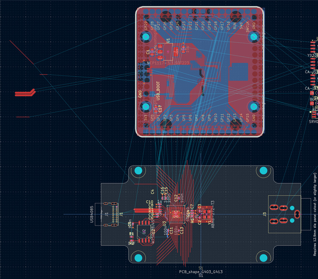
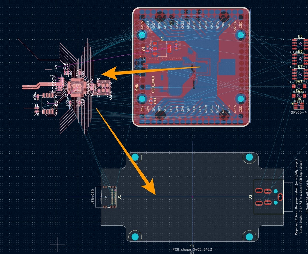
With the schematic updated, I switched to the PCB editor and took a screenshot of the original layout for reference. I then selected the main central portion of the circuitry and moved it onto my new PCB outline.
image

The result looked promising:

image

The original design includes a top-layer +3.3 V copper fill zone, and I wanted to preserve part of that arrangement. To do this, I simply created a new fill zone and roughly followed the outline of the original design, almost like connecting the dots.

image

Once that was done, I moved the new fill zone into its final position. In hindsight, it would have been easier to create the fill zone first and move it together with the rest of the circuitry, but it only took a few moments to fix. The layout was already starting to come together nicely.

image

Next, I selected the voltage regulator section from the original PCB and moved it into the desired location on the new board. Since I no longer needed any of the remaining elements from the original PCB layout, I deleted them. At this point, the project had effectively become a normal PCB design exercise, with the remaining tasks being component placement and trace routing.

image

I’ll write a Part 2 (EDIT: Here is part 2: (+) Getting Custom RP2040 Boards Produced and Assembled with KiCad, Part 2! - element14 Community ) once the layout is complete. I suspect it will be an even shorter post, since everything appears to be progressing smoothly so far.

Thanks for reading!

  • Sign in to reply

Top Comments

  • shabaz
    shabaz 1 month ago +2
    I wonder if the Raspberry Pi people every got one of these PCBs assembled.. they have traces not running through the center of pads. These are lightweight 0402 parts, they will rotate as the solder reflows…
  • arvindsa
    arvindsa 1 month ago +1
    I came here from your Part 2 of this post. Looking at the PCB Layout of the original PCB, I see a lot of polygon on top layer for the 3.3V Net. Now before I say something more, I have to say that I believe…
  • arvindsa
    arvindsa 1 month ago in reply to geralds +1
    I know that the pcb was from 3rd party. I put the question to Shabaz for his take on the originaldesign cos he would have studied the original design with more context. If RPi foundation made it for maker…
  • arvindsa
    arvindsa 1 month ago in reply to geralds

    The USB4930-00-AA is good too specially For Pick and Place machines, this is a better option since there is no compromise on the durability.. Whereas the one I recommended is good for hand soldering. 

    • Cancel
    • Vote Up 0 Vote Down
    • Sign in to reply
    • More
    • Cancel
  • geralds
    geralds 1 month ago in reply to shabaz

    Hi  shabaz 

    Now, I've updated the component USB-C. You have now a SMD variant as well. Alternative I selected is: USB4930-00-AA;

    https://gct.co/connector/usb4930

    The price at Farnel is about 0,460 EUR excl. (10x per pack.).

    https://at.farnell.com/gct/usb4930-00-a/usb-c-buchse-abgew-usb-2-0-16pos/dp/4843852

    Please check this, hopefully this is good for your project.

    Here the created component, both variants:

    USB4930-00-A_GCT.zip

    This type of selection is because it has through holes for the shield as well as locating holes for correct placing the component on the PCB.  

    The variants of the USB's.

    image

    Best Regards

    Gerald

    • Cancel
    • Vote Up 0 Vote Down
    • Sign in to reply
    • More
    • Cancel
  • arvindsa
    arvindsa 1 month ago in reply to shabaz

    Ah, shabaz  Appreciate your views, you've done a thorough analysis, and I see now,  they did add fence around the crystal. That's not a good move from their end. I think what the designers did is they put in the ultra level of best practices out of force of habit for this simple board. Only the circuit is minimalistic not the board layout Smiley

    For the USB-C, My absolute favorite is https://in.element14.com/gct-global-connector-technology/usb4085-gf-a/usb-conn-2-0-type-c-r-a-rcpt-16pos/dp/2924867 , it aint cheap. I do have cheaper option but they are from local stores. but this USB4085-GF-A is something i love because (sorry for the unsolicited opinion)

    1. They are entirely through hole. I can solder it by hand and is not reliant on the PCB's PAD and solder strength. They can take large level of abuse.
    2. The USB has overhangs the PCB and so for case, it is easy to bring the USB flush with the casing without weird design of the PCB
    • Cancel
    • Vote Up 0 Vote Down
    • Sign in to reply
    • More
    • Cancel
  • shabaz
    shabaz 1 month ago in reply to arvindsa

    Hi,

    I agree with your and geralds conclusion, they are not really needed. There's a couple of comments from RPI regarding needing a couple of capacitors very close to the RP2040 (one for 3.3V decoupling, and the other for 1.1V decoupling(, so a bit of supply polygon there can be useful just to practically get more connections to those capacitors, to reduce the series inductance. I don't think RPI did as good a job on the 1.1V decoupling in that minimal board, so I just now modified it slightly. The orange arrows show the pin and capacitor for 3.3V decoupling, and the green is for 1.1V (previously, there was only one connection to that 1.1V decoupling capacitor on each end, now there are three as you can see.

    image

    Other than that, I too don't like having too much unnecessary power planes on top, but on a 2-layer board (especially larger ones) some copper balancing is needed to prevent the PCB curving, so if there are large empty areas I will either tie them to ground, or supply (depending on what connections are nearby). Some people just fill the entire top side with one big polygon, say at 3.3V or GND, which is valid too, but it does visually get difficult to follow traces when troubleshooting. Another option is to fill it all on top but then insert "no fill" keepout rule polygons in dense areas. They can all be valid options, sometimes it's just personal preference.

    I wasn't happy with the crystal footprint, I just now modified that too, with keepout polygons, so that there is never copper fill too close to it since that will just be stray capacitance. I added a bottom-layer keepout too, although probably unnecessary for 2-layer boards. Plus the via fence is likely unnecessary for crystals, but if it were changed to an oscillator module, then it could be helpful to reduce emission. 

    image

    I'll upload these changes to the Github repo, but first I want to make those USB connections in the method that Gerald mentioned. And will also look for an easily-available and low-cost SMD USB-C connector, since it will save a bit of cost during assembly.

    EDIT: also, I will try to find a cheaper crystal, since the one used in the minimal design costs as much as the RP2040 chip.

    • Cancel
    • Vote Up +1 Vote Down
    • Sign in to reply
    • More
    • Cancel
  • arvindsa
    arvindsa 1 month ago in reply to geralds

    Yes, heat does increase with increased frequency. I primarily work with STM32 Series and Nordic 52 and never worked with RP MCUs, So i am following this with curiosity. . The QFN Packages come with thermal pads and their datasheets recommend, it be grounded along with vias to wick the heat to other side.  Also another additional recommendation would be the other side of PCB under the thermal pad (connected via) can be kept without solder mask to improve heat transfer away from the system. But other chips have one thing common, the heat dissipation is via ground or an isolated net.

    And again, You are correct in saying that thermals is something to pay attention to, infact thermals is something many beginners overlook especially the thermal reliefs for each pad. I solder the one PCB using hands with MHP-50. It is a 50x50mm soldering plate and The ground planes do help conduct the heat to other areas of PCB and sort of works like a reflow profile. But it does not work when i have large 3V3 polygons which i use for specific reasons (Switching currents etc).

    It would be interesting to learn if RPi Found a way to improve heat dissipation via VDD plane too. 

    • Cancel
    • Vote Up +1 Vote Down
    • Sign in to reply
    • More
    • Cancel
<>
element14 Community

element14 is the first online community specifically for engineers. Connect with your peers and get expert answers to your questions.

  • Members
  • Learn
  • Technologies
  • Challenges & Projects
  • Products
  • Store
  • About Us
  • Feedback & Support
  • FAQs
  • Terms of Use
  • Privacy Policy
  • Legal and Copyright Notices
  • Sitemap
  • Cookies

An Avnet Company © 2026 Premier Farnell Limited. All Rights Reserved.

Premier Farnell Ltd, registered in England and Wales (no 00876412), registered office: Farnell House, Forge Lane, Leeds LS12 2NE.

Follow element14

  • X
  • Facebook
  • linkedin
  • YouTube