element14 Community
element14 Community
    Register Log In
  • Site
  • Search
  • Log In Register
  • Community Hub
    Community Hub
    • What's New on element14
    • Feedback and Support
    • Benefits of Membership
    • Personal Blogs
    • Members Area
    • Achievement Levels
  • Learn
    Learn
    • Ask an Expert
    • eBooks
    • element14 presents
    • Learning Center
    • Tech Spotlight
    • STEM Academy
    • Webinars, Training and Events
    • Learning Groups
  • Technologies
    Technologies
    • 3D Printing
    • FPGA
    • Industrial Automation
    • Internet of Things
    • Power & Energy
    • Sensors
    • Technology Groups
  • Challenges & Projects
    Challenges & Projects
    • Design Challenges
    • element14 presents Projects
    • Project14
    • Arduino Projects
    • Raspberry Pi Projects
    • Project Groups
  • Products
    Products
    • Arduino
    • Avnet & Tria Boards Community
    • Dev Tools
    • Manufacturers
    • Multicomp Pro
    • Product Groups
    • Raspberry Pi
    • RoadTests & Reviews
  • About Us
    About the element14 Community
  • Store
    Store
    • Visit Your Store
    • Choose another store...
      • Europe
      •  Austria (German)
      •  Belgium (Dutch, French)
      •  Bulgaria (Bulgarian)
      •  Czech Republic (Czech)
      •  Denmark (Danish)
      •  Estonia (Estonian)
      •  Finland (Finnish)
      •  France (French)
      •  Germany (German)
      •  Hungary (Hungarian)
      •  Ireland
      •  Israel
      •  Italy (Italian)
      •  Latvia (Latvian)
      •  
      •  Lithuania (Lithuanian)
      •  Netherlands (Dutch)
      •  Norway (Norwegian)
      •  Poland (Polish)
      •  Portugal (Portuguese)
      •  Romania (Romanian)
      •  Russia (Russian)
      •  Slovakia (Slovak)
      •  Slovenia (Slovenian)
      •  Spain (Spanish)
      •  Sweden (Swedish)
      •  Switzerland(German, French)
      •  Turkey (Turkish)
      •  United Kingdom
      • Asia Pacific
      •  Australia
      •  China
      •  Hong Kong
      •  India
      •  Japan
      •  Korea (Korean)
      •  Malaysia
      •  New Zealand
      •  Philippines
      •  Singapore
      •  Taiwan
      •  Thailand (Thai)
      •  Vietnam
      • Americas
      •  Brazil (Portuguese)
      •  Canada
      •  Mexico (Spanish)
      •  United States
      Can't find the country/region you're looking for? Visit our export site or find a local distributor.
  • Translate
  • Profile
  • Settings
Raspberry Pi Projects
  • Products
  • Raspberry Pi
  • Raspberry Pi Projects
  • More
  • Cancel
Raspberry Pi Projects
Blog Making a Custom RP2040 Project with KiCad, Part 1!
  • Blog
  • Documents
  • Events
  • Polls
  • Members
  • Mentions
  • Sub-Groups
  • Tags
  • More
  • Cancel
  • New
Join Raspberry Pi Projects to participate - click to join for free!
  • Share
  • More
  • Cancel
Group Actions
  • Group RSS
  • More
  • Cancel
Engagement
  • Author Author: shabaz
  • Date Created: 24 Jun 2026 3:25 PM Date Created
  • Views 1320 views
  • Likes 9 likes
  • Comments 32 comments
  • kicad
  • pico
  • rpiexpert
  • rp2040
  • raspberry_pi_projects
  • pi pico
Related
Recommended

Making a Custom RP2040 Project with KiCad, Part 1!

shabaz
shabaz
24 Jun 2026

Partly out of curiosity, and partly to test some aspects of a workflow for other projects, I decided to create a custom RP2040 board. In most cases, there’s no need to do this; it may well be more expensive than simply using a ready-made Raspberry Pi Pico module and mounting it on a custom PCB, while saving a considerable amount of effort.

This short blog post describes how I’m approaching the project. It’s very much a work in progress.

The first thing I did was download the RP2040 hardware design guide PDF, and the minimal RP2040 design KiCad zip file from the Raspberry Pi website and extract and open the design with KiCad 10. This is what the minimal schematic looks like (click to enlarge):

image

The corresponding PCB layout is shown below. My plan is to reuse parts of this design while adapting it to fit the shape and requirements of my own PCB:

image

By examining the minimal PCB layout, it was possible to see that nearly all traces were on the top layer, with just a few on the underside, leaving the majority of the bottom copper being a ground plane.

Next, I modified the schematic by removing the components I didn’t need and adding the functionality I wanted. For example, I removed the pin headers and the Micro-B USB connector, replacing the latter with a USB-C connector. I also added RS-485 circuitry to one of the UART ports, since the board is intended to function as an RS-485 adapter.

You’ll also notice a 10-pin connector that appears to be underutilised. That’s intentional. I plan to route several unused GPIO pins to that connector in case I need them later. I haven’t assigned specific GPIOs yet; I’ll wait until the connector has been placed on the PCB so that I can choose whichever pins are physically closest. Anything that makes trace routing a little easier is worth considering!

image

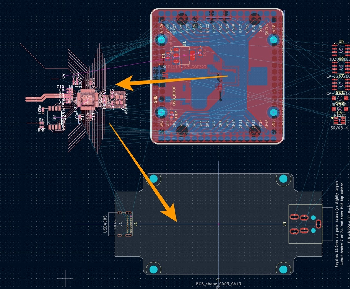
With the schematic updated, I switched to the PCB editor and took a screenshot of the original layout for reference. I then selected the main central portion of the circuitry and moved it onto my new PCB outline.
image

The result looked promising:

image

The original design includes a top-layer +3.3 V copper fill zone, and I wanted to preserve part of that arrangement. To do this, I simply created a new fill zone and roughly followed the outline of the original design, almost like connecting the dots.

image

Once that was done, I moved the new fill zone into its final position. In hindsight, it would have been easier to create the fill zone first and move it together with the rest of the circuitry, but it only took a few moments to fix. The layout was already starting to come together nicely.

image

Next, I selected the voltage regulator section from the original PCB and moved it into the desired location on the new board. Since I no longer needed any of the remaining elements from the original PCB layout, I deleted them. At this point, the project had effectively become a normal PCB design exercise, with the remaining tasks being component placement and trace routing.

image

I’ll write a Part 2 (EDIT: Here is part 2: (+) Getting Custom RP2040 Boards Produced and Assembled with KiCad, Part 2! - element14 Community ) once the layout is complete. I suspect it will be an even shorter post, since everything appears to be progressing smoothly so far.

Thanks for reading!

  • Sign in to reply

Top Comments

  • shabaz
    shabaz 1 month ago +2
    I wonder if the Raspberry Pi people every got one of these PCBs assembled.. they have traces not running through the center of pads. These are lightweight 0402 parts, they will rotate as the solder reflows…
  • arvindsa
    arvindsa 1 month ago +1
    I came here from your Part 2 of this post. Looking at the PCB Layout of the original PCB, I see a lot of polygon on top layer for the 3.3V Net. Now before I say something more, I have to say that I believe…
  • arvindsa
    arvindsa 1 month ago in reply to geralds +1
    I know that the pcb was from 3rd party. I put the question to Shabaz for his take on the originaldesign cos he would have studied the original design with more context. If RPi foundation made it for maker…
  • wolfgangfriedrich
    wolfgangfriedrich 1 month ago in reply to shabaz

    Yes, with full speed USB 12 MHz this is not going to be an issue. For the cost of 1 via you could do the cross-over close to the connector pins and then have a nicer layout all the way into the series resistors, which could be sitting parallel to each other. One of the traces connects the 2 TH pins of the connector on the bottom already, just extend it below the other trace and bring it to the top layer. 

    That is one advantage of the SMD pin USB-C connectors (16 pin without the high speed signals). You can always bring out the D+/D- pair in the orientation preferred by the rest of he layout. They still have TH tabs for stability and should be no problem to solder if you reflow the board anyways. 

    • Cancel
    • Vote Up 0 Vote Down
    • Sign in to reply
    • More
    • Cancel
  • wolfgangfriedrich
    wolfgangfriedrich 1 month ago in reply to shabaz

     if the Raspberry Pi people every got one of these PCBs assembled

    Somebody did this, documented here on Reddit. The pictures are blurry but you can make out C11 on a slight angle with the solder joints still fully on the pads. So this is not going to be an issue other than our need for esthetics. 

    • Cancel
    • Vote Up 0 Vote Down
    • Sign in to reply
    • More
    • Cancel
  • shabaz
    shabaz 1 month ago

    I wonder if the Raspberry Pi people every got one of these PCBs assembled.. they have traces not running through the center of pads. These are lightweight 0402 parts, they will rotate as the solder reflows. For instance, C12 in the screenshot below, would rotate clockwise:

    image

    Here's another unusual trace design, on C14. The left side of it has more copper traces attached to it, it may cause the component to slide leftward.

    image

    I'm going to try to clean these up, because it will get reflowed, I'm not going to hand-solder this.

    For instance, here's a resistor that wasn't in the original circuit. I've brought out both of the traces more aligned, even though it is a longer path.

    image

    • Cancel
    • Vote Up +2 Vote Down
    • Sign in to reply
    • More
    • Cancel
  • shabaz
    shabaz 1 month ago in reply to wolfgangfriedrich

    Hi Wolfgang,

    Thanks! I wanted to tidy it up more, and make that RP2040 symbol more conveniently laid out too, but I didn't change too much for now just in case I ended up accidentally unrouting signals between the original netlist and new, when it came to the PCB.

    I thought it would go easy from now in, but had a bit of minor issues with the USB routing, the RP2040 ordering works best if the USB-C connector is on the underside, which I didn't want to do. I don't have any length matching any more, but it's only running at 12 MHz so it's probably fine over this short length.

    image

    • Cancel
    • Vote Up 0 Vote Down
    • Sign in to reply
    • More
    • Cancel
  • wolfgangfriedrich
    wolfgangfriedrich 1 month ago

    Thanks for connecting the SPI flash and the crystal to the controller chip with wires and not only net labels on the schematic. This way it is much more well-arranged and understandable on first sight. 

    • Cancel
    • Vote Up 0 Vote Down
    • Sign in to reply
    • More
    • Cancel
<>
element14 Community

element14 is the first online community specifically for engineers. Connect with your peers and get expert answers to your questions.

  • Members
  • Learn
  • Technologies
  • Challenges & Projects
  • Products
  • Store
  • About Us
  • Feedback & Support
  • FAQs
  • Terms of Use
  • Privacy Policy
  • Legal and Copyright Notices
  • Sitemap
  • Cookies

An Avnet Company © 2026 Premier Farnell Limited. All Rights Reserved.

Premier Farnell Ltd, registered in England and Wales (no 00876412), registered office: Farnell House, Forge Lane, Leeds LS12 2NE.

Follow element14

  • X
  • Facebook
  • linkedin
  • YouTube