This is the second part of the Eval Kit BD9G500EFJ-EVK-001 RoadTest. If you have missed the first blog, you can check it out here.
In this blog I'm going to design a buck converter to provide power to one servo. Input power is supposed to be 4s LiPo battery pack. With this scenario in mind, the most important feature to me is a fast transient response to limit power fluctuation on the servo. Output ripple is not a main concern.
So, we can define our general specifications:
- 4s Lipo: input voltage from 12V to 17V
- servo supply: 5V output
- servo load: about 3A peak (from experience, will be verified in a moment)
- fast transient response, would be ideal to keep voltage transient less to a couple hundred millivolts
But we don't have to start from scratch!
Luckily, it just happens that I have an evaluation board to assess performances . This makes things quite a bit simpler because we can start from a known performance level and, if needed, improve on that based on the application requirements.
The test setup is extremely simple. Input power supply is set to 15.4V (more or less 50% state of charge for a 4s battery), the servo is connected to the evaluation board output using some solid core wires soldered on the board bottom and the servo signal is generated by a trusty Arduino uno. The servo is controlled such as it moves every two seconds and I can monitor output voltage and current using my oscilloscope.
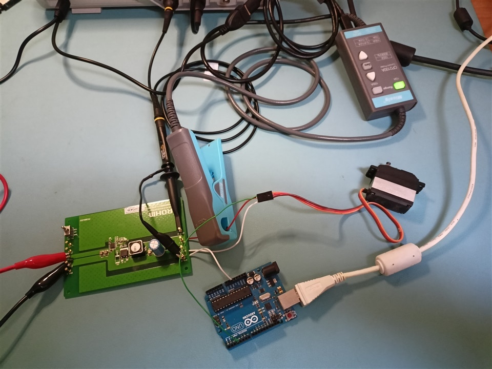 Test setup
Transient response with a servo load
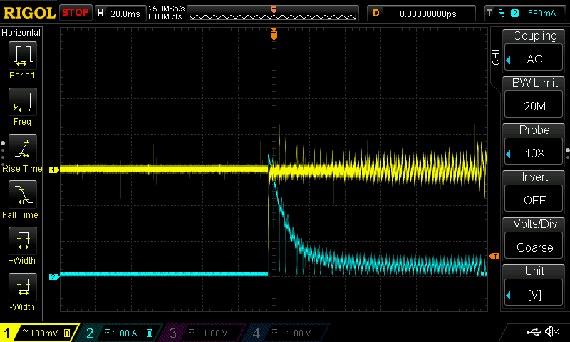
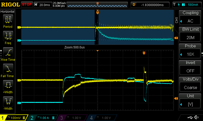
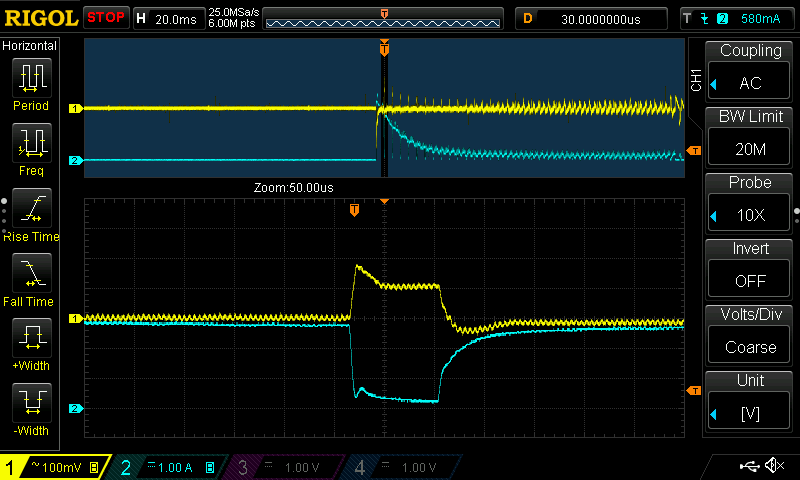
The servo chosen as load is somewhat recent and it's designed to be used on RC planes, but I successfully used it in 1/8 RC cars as well. Its performance is decent, so I expect somewhat high current consumption. This is going to be our starting point and I will use these measures later as a reference.
| {gallery}Initial servo load response |
|---|
|
|
|
|
|
|
Reference transient response using unmodified BD9G500EFJ-EVK-001
This kind of response is already very good and it meets my initial requirements. In fact, output voltage fluctuations are kept to about 200mV even during a 3A load step change. But, even if it meets my requirements, I want to see if I can speed it up even more and I will try to do so in just a moment.
Last torture before the design stage
One feature that I did not test in the first blog is the overvoltage protection, but I'm going to cover it now. In my arsenal I have another servo, but this is an "old style one", designed to be powered up directly by batteries and not by a switching converter. The key difference is that this one, during pwm off periods and maybe even during braking, turns into a generator and pushes back current into the power supply! It can then overcharge output capacitors, making easy for me to evaluate overvoltage protection on the BD9G500EFJ-LA.
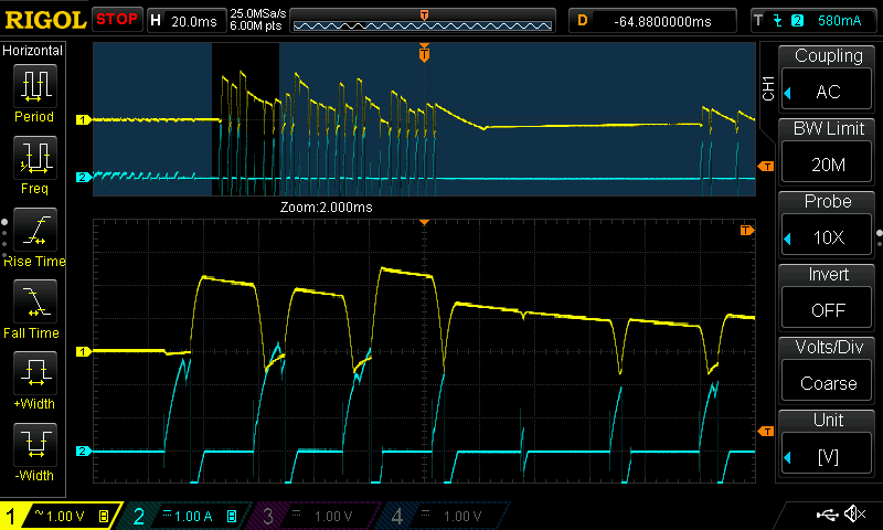 Yellow: AC coupled output voltage. Blue: output current
This image shows what I just anticipated: if you push back current into the output, it will inevitably rise. Here, it went up to 7V. Quite a brutal test!
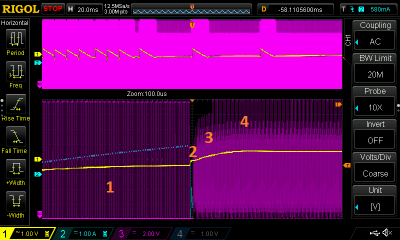
Overvoltage behavior. Yellow: Output channel. Blue: output current. Pink: switching node.
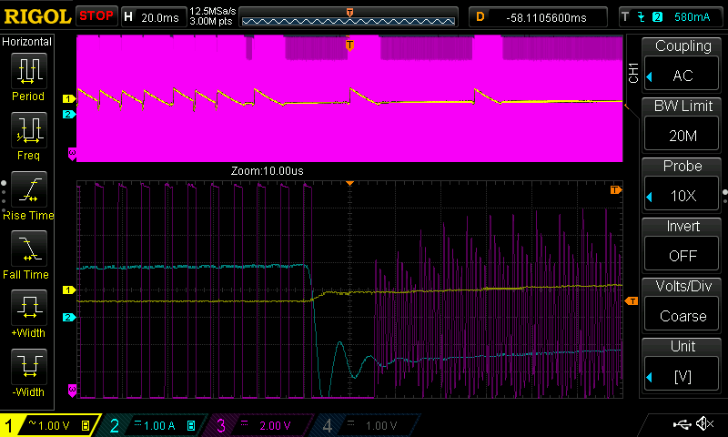
A closer look to an overvoltage event. Notice that the current (blue channel) goes negative., this means that the DUT is pushing back charge
The BD9G500EFJ-LA behavior during an overvoltage event is not that easy to explain, but I hope these images will serve me well. We can define four different phases:
- normal operation: the output current is positive and the BD9G500EFJ-LA is regulating just fine
- current inversion/overvoltage event: the BD9G500EFJ-LA completely stops switching for a brief period
- 100ns discharge mos: the BD9G500EFJ-LA start "pulsing" for 100ns the inductor to ground
- overvoltage discharge: after a predefined number of cycles, the discharge mos pulse duration goes up to 400ns
This behavior matches quite well (except for the "zone 2", which I did not find mentioned) to the datasheet description. On this topic, remain only one thing to disclose: what is all that signal in zone 3 and 4 if the BD9G500EFJ-LA is only switching the discharge mos?
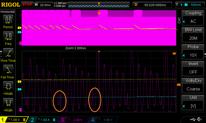 A closer look to transition between zone "3" and "4". Yellow: Output channel. Blue: output current. Pink: switching node.
It's ringing! Here we can clearly see pulses from the discharge mos (the first highlighted pulse duration is 100ns, while the next one is 400ns). The discharge mos, when on, briefly charges up the inductor and when the mos is turned off, the inductor resonates with the rest of the circuit. Parasitics resistance is not enough to effectively dissipate this energy so the ringing keeps going until the next "discharge pulse", when some more energy is fed into the inductor.
In this particular case, a snubber circuit would be beneficial to help the overvoltage discharge function dissipate more energy.
The design process, starting from the BD9G500EFJ-EVK-001
The BD9G500EFJ-LA datasheet, starting from page 17 and going forward, provides plenty of application examples and a good procedure for designing a buck converter.
One thing that caught my eye is the fact that the 5V output voltage reference circuit in the datasheet ever so slightly differs for some components from the evaluation board scheme. This is more easily seen in the frequency response plot for both circuit designs: even if the compensation network is the same, the frequency response seems to be somewhat changed (but not by a lot in the end). The load response in the time domain instead appears identical.
Now, let's begin with the actual design process.
My main goal is to push transient response as far as comfortably possible. To ease up a little the design, I decided to keep untouched the output capacitance (200uF to 250uF is a healthy value anyway) and to increase switching frequency from 200kHz up to 600kHz. This frequency increase allows me to reduce by a factor of 3 the inductance while maintaining the same current ripple. Furthermore, this decrease also helps to improve transient response.
Inductor selection process, as described in the datasheet
For my specific design is not extremely important, but by keeping the inductor ripple current almost the same and leaving output capacitance as designed in the evaluation board the output ripple should be more or less unmodified. If you need to get this argument covered, the BD9G500EFJ-LA datasheet has a whole page dedicated to this design part.
General rules for phase compensation
For phase compensation (the point that I'm most interested in to achieve an even faster transient response) I found the BD9G500EFJ-EVK-001 design very helpful. By "reverse engineering" it and with the help of datasheet's formulas, we can easily find that it uses a crossover frequency (fc) slightly over 10% of switching frequency and a zero point that is lower from the "maximum" fc/9 suggested in the datasheet by quite a bit of margin.
Since the BD9G500EFJ-EVK-001 worked well for me, I will try to keep its design philosophy, just scaling it for my specific use case.
I also have some limitation on the design due to parts I have available, but in the end I modified the board as follow:
- Increased switching frequency from 200kHz to 600kHz
- Decreased inductor from 33uH to 10uH
- Increased theoretical crossover frequency to 64kHz (aiming for 10% of switching frequency)
- Placed zero point around 1.3kHz (aiming for fc/50)
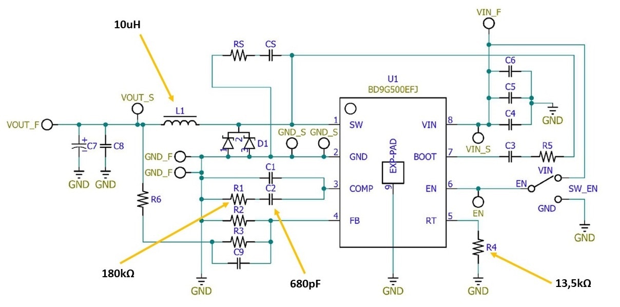
Board surgery
Despite being on the small side, replacing resistors and capacitors on the BD9G500EFJ-EVK-001 proved to be easier than expected: parts are decently spaced apart and soldering pads are quite big compared to component size (0402).
On the other hand, the inductor was quite difficult to remove, mainly due to heavy copper and thick traces that sucked away heat in no time. In the end, using hot air with one hand and a soldering iron in the other, I was able to desolder the inductor.
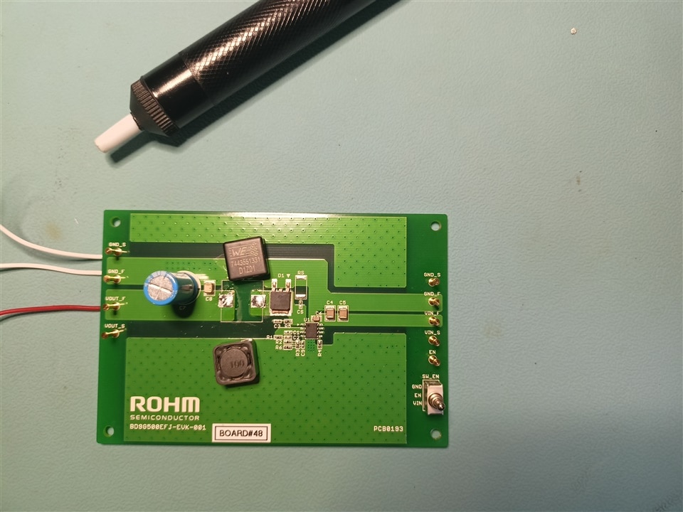 Original 33uH inductor ready to be replaced with 10uH one
New test session with modified BD9G500EFJ-EVK-001
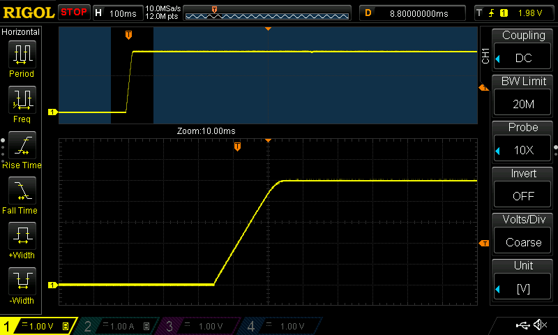 First start up after modding the board
The power up procedure after modifying the board went smoothly, no weird behavior and no instability. Good! Time to test once again the transient response and discover if I've been able to further improve the circuit behavior.
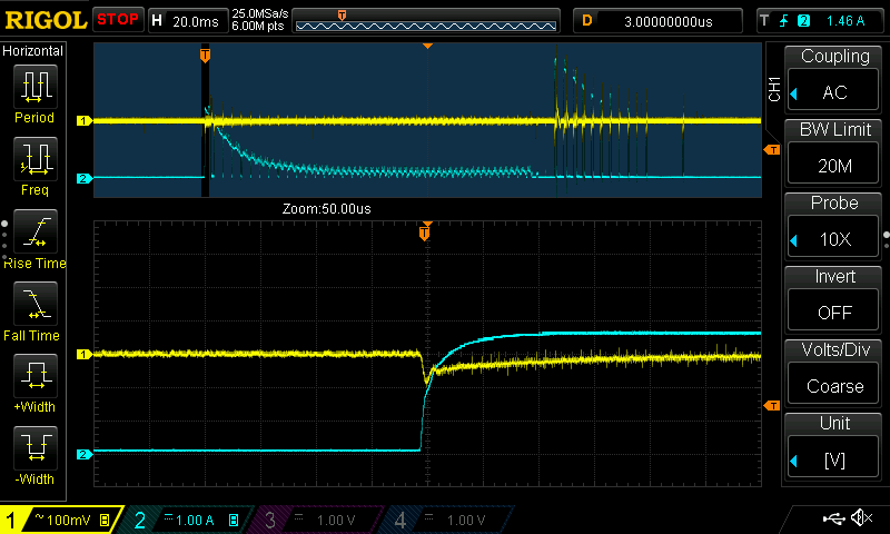
Yellow: output voltage. Blue: output current. Transient response to 3.5A step load
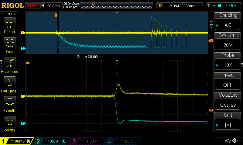
Yellow: output voltage. Blue: output current. 3.5A to zero response
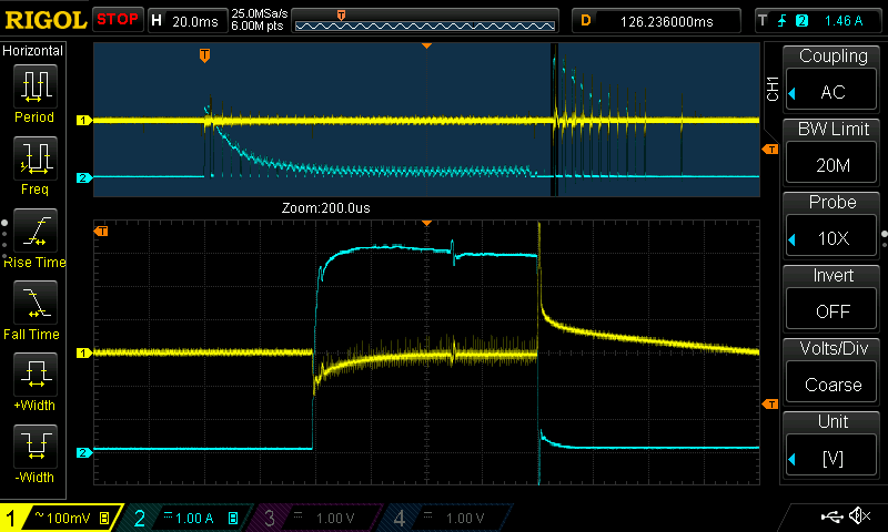
Yellow: output voltage. Blue: output current. Transient response to 6A step load and back to zero
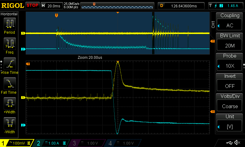
Yellow: output voltage. Blue: output current. Closer look: notice the brief negative current spike
Well, I didn't expect this good of a result. Original BD9G500EFJ-EVK-001 was already impressive, but these measures prove that BD9G500EFJ-LA has an even higher performance potential compared to what is shown (at least for transients).
We started with a peak voltage drop just over 200mV for 3.5A step load and ended up achieving a peak drop less than 100mV for the same step load. Even more impressive, pushing the current demand up to 6A achieved a maximum voltage drop just over 100mV.
Going from a loaded condition to an unloaded one is pretty much the same story, showing just over 100mV peak output increase when going from 3.5A output current down to zero. Short reverse current pulses within a negative going transient are handled extremely well too, as shown in the last image.
Conclusions
Overall, I can say that I'm pretty impressed with overall performances and ease of use. The datasheet has an extensive and easy to follow design procedure and adding to that there are several design examples, including the BD9G500EFJ-EVK-001 one. By utilizing all this information I was able to improve an already good design to tailor it to a specific application with minimal effort and getting things right the first time.
The overvoltage discharge works as described but, at least in my specific scenario, has little impact. This can be likely improved with a snubber circuit.
In the end, the design experience has been very positive and well supported both on the documentation side and on the performance side. The BD9G500EFJ-LA is for sure an excellent buck converter.

