RoadTest: Summer of FPGAs: Microchip Polarfire FPGA Eval Kit
Author: misaz
Creation date:
Evaluation Type: Evaluation Boards
Did you receive all parts the manufacturer stated would be included in the package?: True
What other parts do you consider comparable to this product?: XIlinx Kintex and KC705 Eval Board
What were the biggest problems encountered?: It is impossible to evaluate Ethernet connectivity without paid IP core.
Detailed Review:
I welcome you to this RoadTest review of Microchip PolarFire FPGA Evaluation Kit. I was testing this board for almost 4 month and today I can finally bring this Review. It is incredible board, and it is the most advanced board which I have tested as part of Element14 RoadTest program. Thank Element14 and Microchip for sponsoring and organizing this RoadTest and giving me opportunity to test this board.
This review was sponsored by two companies by sending me their products for free. I would very like it thank Microchip for sponsoring this RoadTest as part of which I received this fantastic FPGA for free.

Second company which sponsored me by sending free part is Samtec. They send me free sample of high-quality high-speed PCI express extension cable PCIEC-064-0500-EC-EM-85 which I used when evaluating PCIe connectivity of FPGA. This cable allowed me to use board outside of computer.

In this RoadTest I decided that I will write TLDR summary and score at the beginning of review. If you are interested in more details, then just continue reading below this table. My review is very detailed (and long), so for readers without sufficient time to read it completely here is short summary containing my main findings.
|
Category |
Pros |
Cons |
|
FPGA |
|
|
|
Evaluation Kit |
|
|
|
Development Environment |
|
|
|
Documentation |
|
|
Product Performed to Expectations: 4 because I was unable to test Ethernet connectivity because some required IP cores are paid.
Specifications were sufficient to design with: 4.5/5 because after migration from Microsemi to Microchip it is hard to find some demo guides and many links in PDFs are broken.
Demo Software was of good quality: 5/5. Tutorials are very high quality.
Product was easy to use: 5/5. I did not face any significant issue. Microchip offers lot of tools simplifying development.
Support materials were available: 5/5. I do not remember any situation when I needed any support.
The price to performance ratio was good: 5/5. Price to performance ratio is better than in case of Xilinx. Board and FPGAs are much cheaper than Xilinx competitors which gives you only few benefits over PolarFire.
Unboxing of the board I described in dedicated blog post which I wrote after I received the board. It contains some basic information about board package, description and my first design.
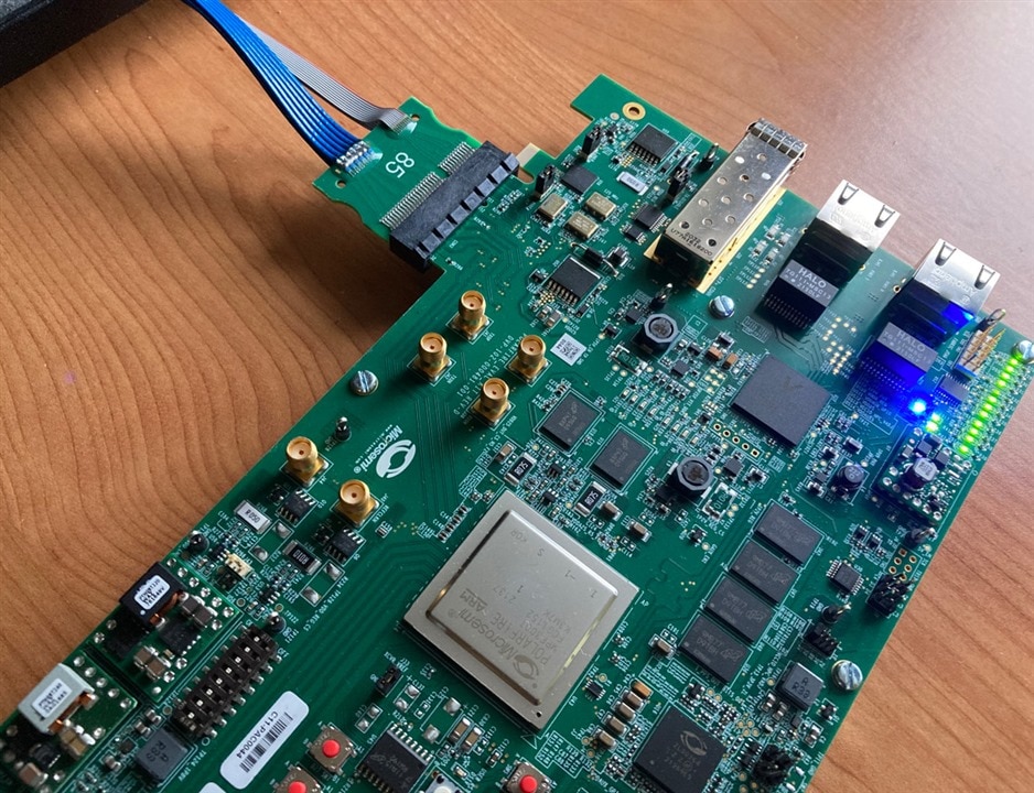
At the beginning I would like to explain what this review is about. It is about Microsemi PolarFire FPGA Evaluation kit which is development board featuring very powerful and large FPGA which is chip with programable logic array which you can use for running your own logic circuits. Following image show the development board:
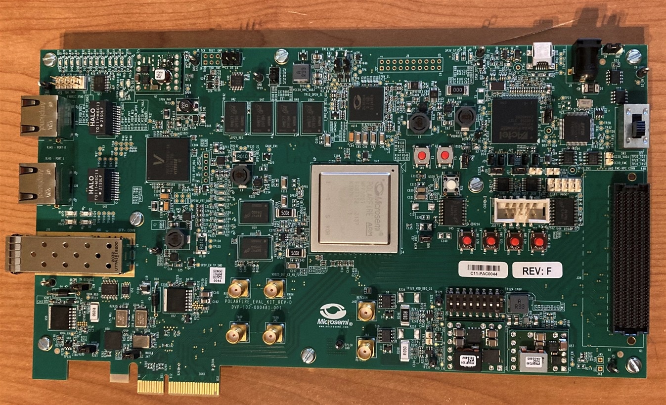
Board reviewed in this review and shown on photo above is great. It is one of the boards used for evaluating PolarFire FPGA. History of PolarFire FPGA is long. Currently this division is as part of Microchip company and nowadays most information and documentation related to board is at Microchip website. Historically this division was part of Microsemi company which was acquired by Microchip. The board was designed in the era when Microsemi was independent company, so board and main FPGA chip contains Microsemi logo. If we go deeper to the history, we can see references to the Actel company. After googling I found that historically FPGAs were developed by this company which was later acquired by Microsemi. In fact, this board has two FPGAs. One of them is main PolarFire FPGA and second one is supporting SmartFussion FPGA which is mainly used for power monitoring. If you look at SmartFussion FPGA which is near right top corner you can see Actel logo on it.
Microchip offers FPGA in many families. PolarFire is splitted to two families FPGA and SoC. FPGAs are chip with configurable fabric but no hardened processors and SoC familily has similar fabric but also there is hardened high-performance CPU. In comparison with Xilinx Microsemi did not hardwired ARM CPU, but instead they hardened modern RISC-V core. But this is not this review about, because this review is about FPGA family which has no dedicated processor. If you want to integrated processor in your design, you can use soft cores implemented in logic fabric as I will describe later.
Microchip offers multiple Development Kits for evaluating this family of FPGA. They are listed on Microsemi webpage. Note that at the time of writing this review there is confusion because some information are available at Microsemi website and some were moved to Microchip Website. Similarly, there is confusion with Application Notes renumbering. There are three evaluation Kits from Microchip (and some other from other companies) named Video and Imaging Kit, Splash Kit and Evaluation Kit. Kits differ in offered features, peripherals and expansion connectors and of course they (significantly) differ in price. This review is about Evaluation Kit. Video and Evaluation Kit use the same FPGA but Video Kit has two cameras, two HDMI connectors, display connector and MIPI CSI-2 connector. None of these is available on Evaluation Kit. In opposition Evaluation Kit (described in this review) has many other interfaces including 3 ethernets (Video kit has no Ethernet), PCIe, exposed high-speed differential signals using SMA connectors and has more onboard peripherals including better RAMs, FLASH memories and secondary FPGA for power measurements. Splash Kit is younger brother of Evaluation Kit. It has FPGA with the same size of logic fabric but less pins exposed from package. It has one Ethernet connector (Evaluation has additional one and one for 10GB Ethernet). Splash fit also includes secondary FPGA for power measurements and PCIe connector like Evaluation Kit. Splash Kit is cheaper and smaller. I personally think that for getting into the PolarFire and for learning it, it is better to start with Splash Kit rather than full Evaluation Kit. There are many similarities in these boards.
Board contains tons of parts and chips. It is one of the most advanced development boards which we have seen in RoadTest program on Element14 in last years. Schematics of board is available but note that available is only schematic of board revision D while for a review I received board revision F. There is available Product Change Notice describing difference between revision D and E but I have not seen described changes in revision F anywhere. Changes between revision D and E are sad. Microchip in this revision change replaced DDR3 RAM (note that Kit has two types of RAM memory, there is memory 4GB of DDR4 RAM and 1/2GB of DDR3 RAM). They changed type of DDR3 part used but they reduced memory from 2GB to 1GB. This is very important change which may affected someone whom design worked on boards rev A to D but do not work on newer units (rev E and later).
Except two FPGAs and RAMs described above another important onboard chip is duel 1GB Ethernet PHY used with two RJ45 jacks for Ethernet Connectivity. It is VSC8575 and also comes from Microchip (originally Microsemi). Except 1GB Ethernet there is additional SFP+ cage for interfacing with other high-speed boards or 10 GB Ethernet. Except chips described above there are tens of other supporting chips including many voltage regulators, modules, level shifters, transistors and so on. According to available BOM spreadsheet there are 78 components marked by U reference designator which is used for naming chips on board. Board has 1828 components in total according to documentation (I did not count them all for checking :D). As a consequence it is hard to search for example jumpers.
From previous description you can deduce that this review is about very complex and advanced board. Now let’s look to the competitors for a while. Biggest competitor for onboard FPGA (which I will describe in detail later) is Xilinx Kintex which is offered in a variant with similar properties. It also has evaluation board referred as KC705. This board has similar peripherals and components. It has one more HPC FMC port for extension. It has twice more PCIe lanes, HDMI output, SD card slot and display. But KC705 Evaluation Kit has only one type of memory. It has 1GB of DDR3 while PolarFire Evaluation Kit has additional 4GB of DDR4. In opposition KC705 has RAM in SODIM socket, so you can replace it. In case of PolarFire evaluation Kit you can’t do this because all 5GB of DDR3 and DDR4 RAM is soldered on board. KC705 has only one 1GB ethernet (PolarFire evaluation Kit has two) and also has no power measurement circuit. Except these differences they look similarly and target similar segments. Big disadvantage of KC705 board is price (this also apply to FPGA as I will describe later). It cost about 800 USD more than PolarFire Evaluation Kit.
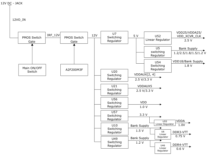
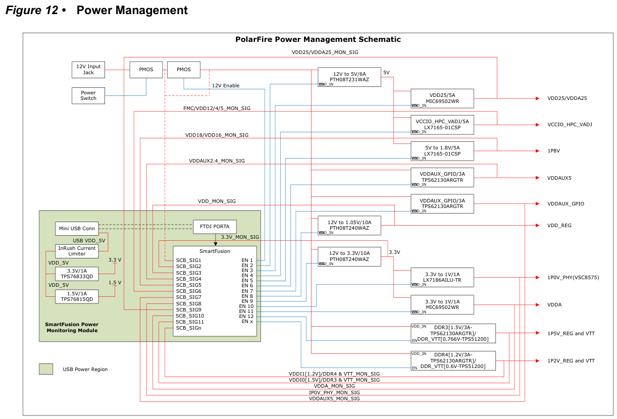
Board powering scheme was a little surprise to me and at beginning I was not sure if some parts are not back powered somehow but later, I found in documentation that my connection and board powering was correct. Board is powered by 12V source. It can be provided using barrel jack from adapter which is bundled in package or using PCIe connector. Board has big switch for powering it on or off from 12V barrel jack source. Turning switch on does nothing which surprised me for a first time. You need to connect USB connector from computer. In opposition when you turn switch off, some part of board remains powered from computer. It makes sense but requirement on connecting PC surprised me when I was powering board first time. I originally used following diagram from datasheet for reference of board powering:
But later I found in the same document more detailed schematic which includes and highlights why USB connection is needed:
The biggest issue of the board I feel lack of standard 2.54 mm pin headers for connecting external components. There are only 6 pins exposed on one pinheader and few other can be abused from other peripherals and features but only way how to get GPIOs for general purpose is using HPC FMC expansion card. Because I am hobbyist 2.54mm pinheads are quite important to me, but lack of them is acceptable from this high-end evaluation board, I think.
For now, I will close description of board and move to describe main FPGA on this board.
Onboard FPGA is MPF300TS-1FCG1152I. MPF means Microsemi PolarFire FPGA (other options are MPFS indicate PolarFire SoC and other identifiers for other families), 300 indicates approximately 300 000 of Logic Elements (other options in PolarFire family are lower 050, 100, 200 and higher 500), T indicates available Transceivers and S Indicates availability of Security Module. Second part of name indicates speed grade (-1), package of the chip (BGA with 1152 pins), and industrial temperature grade (-40 to 100°C).
From the previous description you can deduce that FPAG used on evaluation Kit is one of the best in family and allows you to evaluate almost everything what this platform offers. If your design for some reason overflows 300 000 logic element (or other resources) you still have chance to upgrade to 500 000 unit. Differences between families nicely highlights table from Microsemi website:
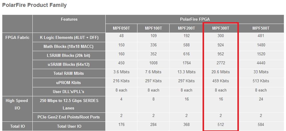
As you can see, they offer less models than for example Xilinx does, but I do not consider this as an issue.
FPGA fabric is built from Logic Elements which are basically 4-input lookup tables (LUT) with Flip Flops. They are chained for easier implementation of circuit used for binary addition. Logic elements are slightly less capable than logic elements available in biggest competitor Xilinx Kintex FPGA which has Logic elements featuring 6-input LUT possibly configurable as two 5-input LUTs. This also means that comparing number of logic elements is not very clear because Xilinx FPGA with the same number of LUTs will be more flexible and synthesis of the same design most probably will on Xilinx FPGA consume less logic cells for the same design. In opposition hierarchy in PolarFire FPGA is simpler and it is easier to understand. I personally think that structure of some parts of Xilinx FPGAs is very complicated. There are slices, CLBs and so on. In case of PolarFire FPGA there hierarchy is described as large field of LEs and other parts (which I will describe later) glued to the array of 36 LE.
Logic elements are surrounded by memories and match blocks (DSPs). There are 4 types of memory:
From practical point of view there are multiple ways how to use this memory. You of course use them directly in block design or VHDL and directly connect signals to them, but you also can use comments near vectors in Verilog and VHDL codes and then Synplify (which is used for synthesis in Libero SoC IDE) will connect these memories automatically for you reducing number of registers implemented in fabric.
While these memories are here, they are used very rarely in demo projects because evaluation board has DDR3 and DDR4 memories (5 GB in total) and most example projects from Microsemi use these DDR memories instead of using local memories. It is quite funny to me that they use 1GB RAM for storing ~2KB of firmware and ~4KB of runtime RAM for soft core demonstration project. It is most probably because DDR controller is easier to connect to the AXI bus.
PolarFire FPGA has Math Blocks which are similar to DSP blocks on Xilinx Kintex FPGAs. DPS in Kintex is slightly more powerful. While internal structure is very similar to math block on PolarFire Kintex mainly support wider operands.
As you can see fabric is slightly less flexible as a fabric from Xilinx but is easier to understand and because most of things is handled by synthesis which can bypass some limitations, then it does not have significant impact on you. I guess that you will feel that blocks in complex designs exhaust slightly faster than in case of Xilinx FPGA but I think that PolarFire FPGA fabric is still suitable for any standard use case and in most case you will not feel differences.
Except fabric FPGA has many peripherals hardwired and connected to the fabric. These peripherals are mainly Transceivers which supports transmission serialized data on speeds between 250 Mbps and 12.7 Gbps. They are used for serializing and deserializing data to/from the fabric and they are used as part high speed interfaces which are available on RoadTested evaluation kit. They are core peripheral for implementing PCI, Gigabit and Ten Gigabit ethernet connectivity which are supported on this board. Competitive FPAG from Xilinx has similar transceivers which supports speed up to 12.5 Gbps which slightly less but almost the same in general. Differences are on PCIe side. Xilinx Kintex supports only one PCIe port while MPF300TS supports 2 PCIe ports but Kintex supports using up to eitght lanes while PolarFire only 4. Note that PolarFire’s 4 PCIe lanes are shared between two ports, so you can’t use both PCIe ports when using 4 lane setup. This limitation is described in User Guide in note:

Another interesting part which is present on PolarFire FPGA is security engine. While Xilinx support encrypted bitstream I never heard about security (not only crypto) engine on Xilinx Spartan to Virtex platforms. Engine present on PolarFire FPGAs with S letter in name supports many interesting security features including digitally signed certificate of every manufactured FPGA for preventing using counterfeit FPGA, Physically Unclonable Function (PUF) and also licence for using patented side-attack resistant implementation of cryptographic engine in fabric. Except these unique features it has standard crypto features which you may know from advanced MCUs like True Random Number Generator, Secure Key Storage (write only keys), accelerators for symmetric encryption (AES), asymmetric cryptography (RSA, DSA, ECC) and hash computations (many SHA algorithms are implemented). All these engines are resistant to DPA side channel attack according to documentation (I did not check on this). All these features are described in available User Guide. It is nice because most vendors release information about security features only under NDA. Microchip did not go this way and instead they publicly described all implemented security features. This FPGA looks very interesting when you are interest in security and need it in your application. Mentioned User Guide is very interesting, and I recommend reading it even you do not plan to use PolarFire FPGA because it mentions many advanced security features, attacks, and mitigations. It is good to know about these security aspects.
GPIOs of PolarFire FPGA are grouped to two groups – GPIO (General purpose) and HSIO (High speed). High-speed are used for connecting fast signals like DDR RAMs. GPIOs support more feature and higher voltages but are more speed restricted.
Now let’s close mostly theoretical description and some comparisons of this powerful evaluation kit and its FPGA and go to something more practical.
Libero SoC is tool which you will spend most time in. Equivalent in Xilinx world is Vivado.
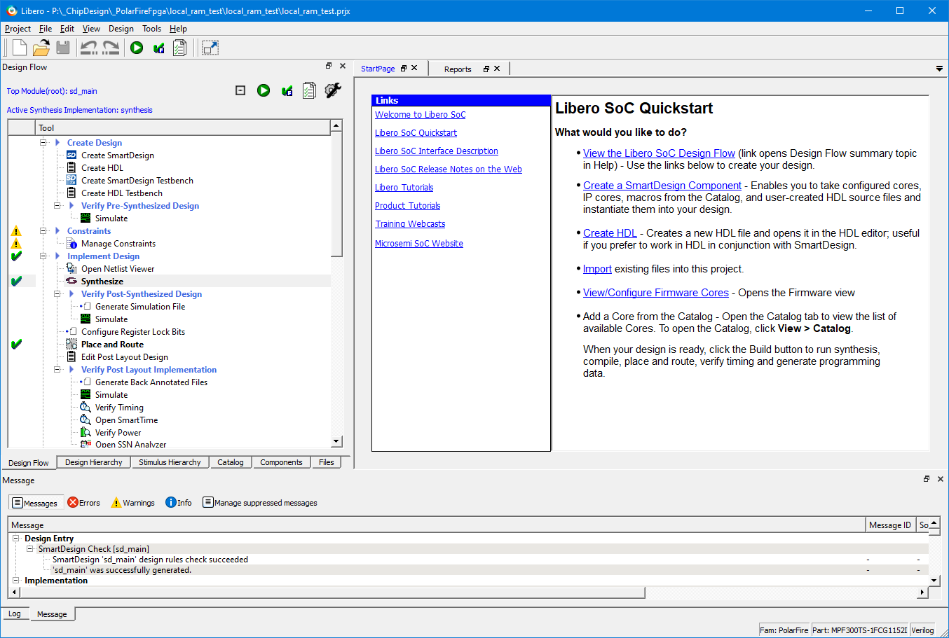
In comparison with Vivado this tool looks older. It looks quite outdated, but it is practical, compact, and fast. I like it for this reason. To be frank I don’t like Vivado very much because it is slow to me, every click in Vivado has long delay and many error messages from Vivado (which occurs frequently) has no (usable) description and you must search for description in some Log, Messages, TCL console, other windows and most of time also on internet. In these terms Libero SoC is much better. Libero uses single view and single layout and do not switch layout when working. When I began with Vivado I was scared by changing layout when switching between modes and I was unable to find window which I have opened few minutes before. Here in Libero, it is much easier and intuitive to me. Libero is only GUI and internally runs other commands for achieving tasks. This is similar to Vivado. Many (important) parts of design process were not implemented by Microchip, but some of they were outsourced. As a example we can use synthesis and simulation. For synthesis Vivado uses Synopsys Sinplify and for simulation Mentor ModelSim is used. These tools are licensed and you get OEM license as part of Libero licenses. This also apply to free silver license which I use. Synopsys Synplify licenses still mention company name as Actel which indicates that history of this toolset is long (Actel was acquired by Microsemi and Microsemi was acquired by Microchip as I mentioned at the beginning of this review). Licensing is strict and according to documentation prohibits running in Virtual Machines. I have not tried running it in VM, but I faced licensing errors when I want to work remotely over Remote Desktop. In this case synthesis failed with error. This is sad, especially in post-covid home-office era when many workers work from home over Remote Desktop.
Work in Libero is easy. I did my first design without using any documentation and tutorial. I had experiences from Vivado, so design flow was not totally new to me, but in summary, it was easy to adapt to Libero SoC. Later I tried follow tutorial for developing systems with RISC-V Soft Cores and in this tutorial TU0775 I learned some other features which I skipped or missed in my first design. I recommend read this and other tutorials from Microchip, they are very nice. Most of them is outdated a little and Libero contains some new buttons or default value of parameters mentioned in tutorial changed but in overall, they are very useful.
Libero follows similar design flow like Libero, but you can skip some steps which Vivado forces you to do. For example, in my first design I did not run any verification (because I of course did not write testbench for my LED blinking project) and I also did not run timing verification (I assumed that so powerful FPGA will have no issue with circuit clocked at 2MHz :D). First step is writing HDL codes and possibly creating block design. While you can design your design in a way without any block design, I recommend using block design at least for configuring clocks, resets and initialization complete indication logic.
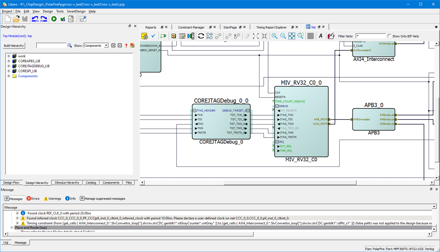
Verilog/VHDL editor in the IDE is available with basic code completion and syntax highlighting. I missing snippets feature which is available in Xilinx Vivado. Editor is simple but when writing large number of codes, I preferred writing them externally in Visual Studio Code and do only minor edits in Libero. The same I do in Vivado because editor in both IDEs are very simple to me, and I like advanced features which offers VS Code with corresponding plugins.
After completing your design, you need to generate component from block diagram. This is done by Vivado at the background. In Libero you have to do this manually. Then you need to select root component and after this you can proceed to synthesis. Synthesis is done by external tool from Synopsys. My feeling from this tool was that is very fast. Synthesis in Vivado takes much more time. I did not measured durations using the same HDL files, but my personal feeling was that it is about 2× faster than synthesis with default strategy in Vivado.
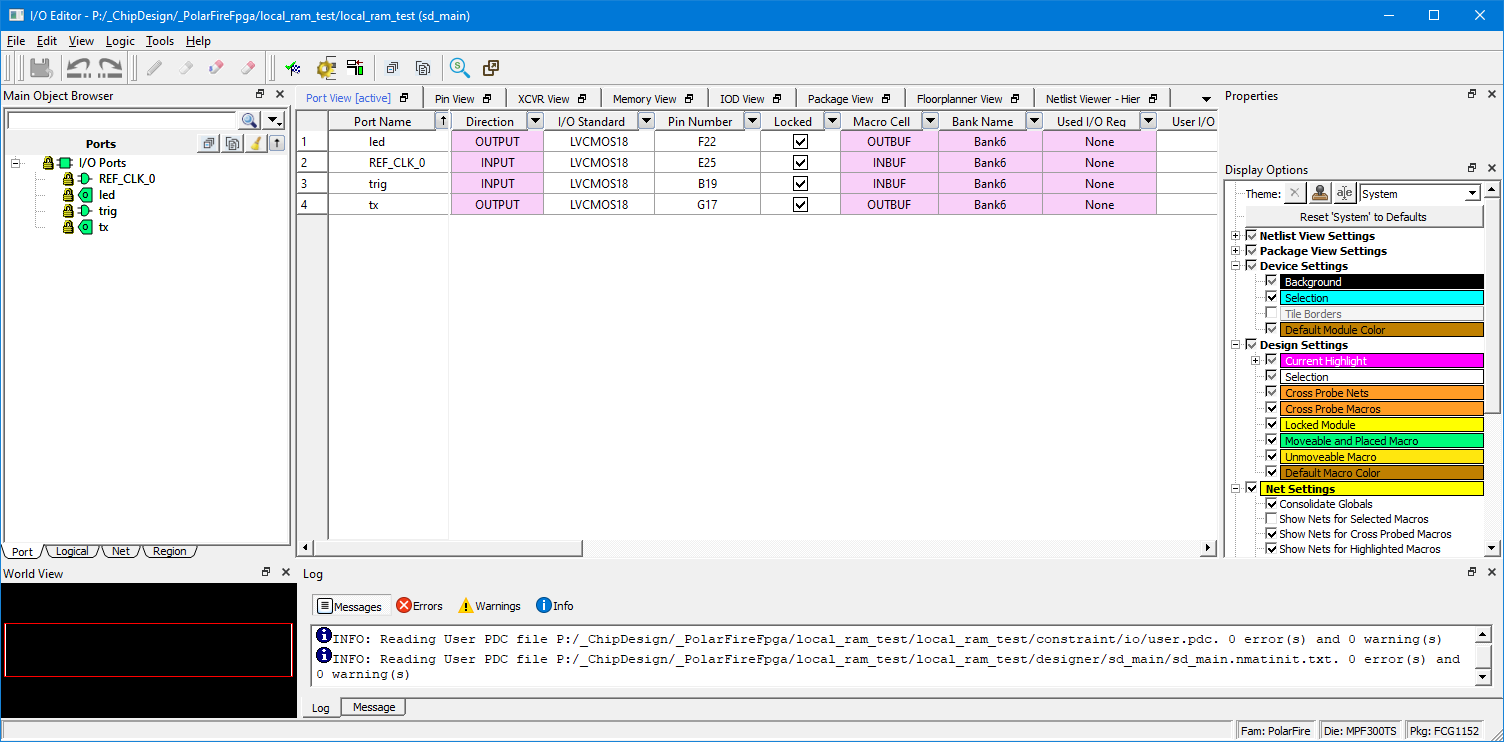
After synthesis you can define constraints. It took me a while to learn this. For defining pinout, you can use GUI tool which will generate IO constraint file for you.
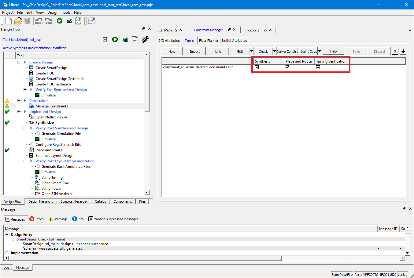
On Microsemi platform timing constraint are separated and usually defined in another file. Libero has very nice feature for extracting timing constraints from block design. Tool will load your design, search for any clock macros and blocks including blocks with derived clocks and generates constraint file. Then you can mark for which parts of design process you want to use specified constraint file and possibly use different constraint file for every step. I have never seen this option in Vivado but most probably there is some way how to do the same in Vivado and I just do not know about it.
After defining constraints, you can run place and route step. Place and Route is seamless step, and I never faced any issue or error from this step. The only issue was that it run long on one design. I will write about it in PCIe section later. Then you can start generating bitstream and possibly also data for SPI flash memory with other initialization data. For some reason building bitstream and initialization data take very long time. After it completes you can run PROGRAM action which will program your device. There is big difference with Xilinx FPGAs. PolarFire FPGA is flash based FPGA while Xilinx FPGA is RAM based. When you program your Xilinx device from Vivado and then reset it, your design is lost, and you must program it again after boot (or store it in external FLASH from with FPGA will load it in initialization time). In case of PolarFire FPGA design is stored in flash and is loaded at initialization time. In opposition programming FLASH memory takes (significantly) more time than programming SRAM cells, so programming FPGA from Libero takes much more time than the same action takes in Vivado.
The disadvantage of Libero SoC IDE is that it has no integrated simulator and for example cannot view signal plots from simulation like Vivado does. When you click simulation step It will open ModelSim GUI (which looks even more outdated than whole Libero) but it is also professional grade tool which you receive (usually expensive) license for free as part Libero SoC for use with PolarFire devices. I used this tool at university, and it is complicated to me. It is also slow and not very user friendly but supports all features of UVM library and as I have heard it is industry standard for verification.
As I have mentioned at the beginning, I consider error reporting in Libero more user friendly than in Vivado, but I still faced some crazy errors when developing my testing designs. The most annoying error was error saying that I have selected non-existing FPGA. This error sometime appeared from GUI and sometime in log from design flow steps. Resolution was always to restart Libero and rerun action.
![]()
To summarize I like this development environment. While it has some disadvantages and some outsourced tools are less user friendly, I still like it more than Vivado mostly for more performant GUI with simpler layout, better error reporting and links to documentation and help.
Microchip offers many documents ranging from brochures and whitepapers to very detailed user guides describing hardware in very deep level. All documents are available as PDF. As I already mentioned there is confusion caused by acquitision of Microsemi by Microchip. Originally all documents were on Microsemi website, and they were organized in groups in compact list all on one page. On Microchip webpage you need to searching multiple categories. But Microchip website contains newer revision document so pay attention when downloading document from old Microsemi website and rather check for the same document on Microchip website.
Microsemi do not produce one very long reference manual like Xilinx do it. Instead, they produce single topic relevant shorter PDFs about 100 pages long. It is named as a User Guide (UG). In these documents you can read very detailed description of hardware, hardwired blocks of FPGA and also about advanced and unique features of FPGA. Because It is split to multiple documents it is hard to check that you downloaded all user guides for all parts. Especially It is complicated because on Microchip website they are mixed with other documents named as user guide, but I think some of them should be named application note. On original Microsemi website there were demo guides which I consider as a tutorial. They are also available on Microchip website, but they are renumbered. Another caveat of acquisition is that links in PDF documents to Microsemi mostly do not work anymore. For example, in already mentioned tutorial TU0775 is linked to download demo files, but link is broken. Because I did not know about structure and location of newer renumbered application notes It took me 15 minutes to find it. I am not sure, but I feel that some files disappeared completely.
Microsemi provides two very detailed step-by-step tutorials describing integration of soft cores to design and showing both hardware and also firmware part. One tutorial is designed for use Mi-V core which I will describe later, and second tutorial shows similar design using AMR Cortex-M1 core. Both tutorials are nice and can learn you all required for master Liber SoC and SoftConsole (which is Eclipse IDE for softcore firmware development. I will describe it later).
The very good part is that documentation is directly linked in Libero SoC. It is very useful in case of IP cores. It was useful when I used some core first time. Microchip produces document with signal and options description. It is linked directly in IP catalog which is very nice.
My only notice about documentation is that screenshots of block diagram in documents (and mostly tutorials) are very low resolution. They are often significantly zoomed out, so screenshot miss many descriptions and is very hard to flow signals on block diagram screenshot with blurred lines without signal descriptions.
Microchip offers several easily-integrable soft cores on their platform. They support:
As part of review, I learn and tried using Mi-V and CoreABC. I did not try proprietary Cortex-M1 core, but it is also possible and there is tutorial how to use it on PolarFire FPGA. Similarly, I did not try use RISC-V implementation from SiFive.
The main soft core for implementing part of design which can run sequentially and do not need acceleration on fabric is Mi-V. it is CPU core implementing open and modern RISC-V instruction set. There are five Mi-V processors implemented with different instruction set extensions. Implemented extensions are:
There are four cores available in configurations MAF (with L1 cache and AHB system bus), MA (with L1 cache and AHB or AXI system bus) and one MC core. Except these there is newer more optimized version of core which can be configured for options M, C and MC. All these options are freely available as part of Libero licence, and you can freely use them in design. They are available with full Verilog RTL, so you can view their sources and possibly edit them (I did not check, but maybe some licence restriction applies for edits). You can configure many properties of the CPU and optionally integrate (or remove) optional features of the core. For example, you can configure number of external interrupts which you want to connect to interrupt controller of this soft core. Following screenshot show configuration dialog of newer Mi-V core. Older cores with L1 caches are fixed and their configuration is mostly static. As you can see there is help icon near to every field which. After moving mouse to the help icon, you will see tooltip with brief description about related feature and its meaning.
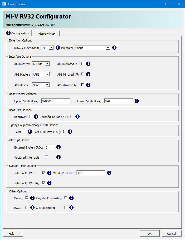
After placing to the block diagram, connecting clocks, resets, interrupts, bus interconnects, slaves and memories, then you can synthetize your design. Process is quite seamless. Especially because of availability of nice step-by-step tutorial. After deploying you can start SoftConsole IDE and start developing your firmware. SoftConsole is eclipse based IDE with bundled GCC toolchain supporting compiling firmwares for RISC-V instruction set. Implementation done by Microchip is minimalistic and it is almost pure Eclipse. There are no templates, and you will need to start from empty project. Empty project is realy empty and there is nothing. You will need to manually write (or import from example projects) Makefile, assembler startup files, linker scripts, debug configurations and all these configure from scratch. I recommend following tutorial TU0775 which show minimalistic but very useful way how to write, setup and compile firmware for Mi-V CPU. Good is that you are able to deploy firmware to the Soft Core running on FPGA directly from FPGA and you do not need to synthetize whole design after any (firmware) modification.
Expect Mi-V core there is another interesting (free) soft core from Microchip. It is CoreABC. ABC is abbreviation of APB Bus Controller. APB bus is bus used for connecting lot of peripherals to the AHB/AXI bus (you need bridge between AXI/AHB and APB). You may also know it from the microcontrollers. CoreABC is very small core. According to documentation it can occupy as small as 101 Lgoic Elements according to documentation. My design with UART controller, Reset and clock controller consumed 434 Logic Elements (0.14% of device capacity). So, as you can see it is very minimalistic controller. This core is very simple CPU core able to execute basic programs. Programs are written directly in assembler and there is no compiler, but there is no need for it. Documentation to the assembler is directly linked in IP Cores catalog. From documentation you will easily learn how to implement core and how to write its firmware. Firmware can be hardwired (434 Logic Elements utilization included embedded firmware!). Instruction set covers basic instructions and also instruction for accessing APB bus. After you learn basics, then using this core is super simple. Controller is configurable. You can configure many parameters like bus size, maximum number of instructions (program counter width), number of IOs and Interrupts and many other. Firmware you can type directly in configuration dialog. Configuration dialog is very smart and don’t allow you to confirm it when something is wrong. It checks your typed firmware and checks parameters. If it finds any mismatch (for example you configure core to 8-bit data bus width and in code you attempt to load constant higher than 255), then dialog will indicate this error to you and will not allow you to confirm the configuration dialog. Controller is very simple. It is triple-cycle CPU. Every instruction (arithmetic, jump, …) take 3 clock cycles. Only exceptions are instructions issuing transactions on APB bus which takes 5 clock cycles. The only issue is its name. Searching for CoreABC on Google produces lots of meaningless results. Searching for just ABC produces even more useless results.
Soft-cores ecosystem I consider more polished then in Xilinx world. RISC-V cores are very versatile, but competitor MicroBlaze is slightly more configurable. Super cool is CoreABC which can be used for minimalist controlling of peripherals and GPIOs. It is very simple and consume virtually nothing on the FPGA fabric. I do not know about any alternative to this controller in Xilinx world.
Flash & freeze is very interesting feature of PolarFire FPGA designed for lowering power consumption. Purpose of this feature is that FPAG store some information like state of GPIO pins in Flash memory which allows to power off some part of logic (powering off logic significantly reduce power consumption). This description is as it was described in brochures about one year ago when this RoadTest was opened, and I was researching about it. Currently it is almost impossible to use this feature. Microchip for some reason remove all references to this feature. Feature was triggered using system services block which is hardwired block with APB interface and can control some core services of FPGA like In Application Programming, some security features, and so on. I have seen some demo design (currently application note) regarding system services which in history contained option to test flash & freeze but later this option was removed from demo and currently available Application Note and related demo project files do not contain any reference to Flash & Freeze. I think they maybe find some caveat (maybe limited write cycles of FLASH memory?) and for this reason stopped recommending using this feature. It is possible that this feature maybe returns sometime in the future. Technically it is as part of FPGAs but without documentation and demo design it would be very tricky to use it. I did not try it.
PolarFire FPGA supports many interesting High-Speed Interfaces which are mostly implemented using High-speed transceivers which support speeds between 250 Mbps to 12.7 Gbps on PolarFire FPGA. As I mentioned at beginning RoadTested Evaluation Kit support evaluating many of them. At the time of applying for this RoadTest I was mainly focused on high-speed gigabit ethernets, and this was one of the features which I attempted to test it first time after I received board, but I “failed” very soon. The issue is that for building design with ethernet you need to use CoreTSE IP Core which is paid . CoreTSE (TSE means Tri-Speed Ethernet) is not hardwired block. Hardwired transceivers are of course available freely to use in designs. CoreTSE is block for processing data from these transceivers and implements Ethernet MAC layer as defined in 802.3 standard. It is also available in variant with AHB bus interface instead of pure signals of MAC data path interface. To summarize there are two variants of CoreTSE available: CoreTSE and CoreTSE_AHB.

In Libero they are indicated by yellow key sign which incates paid license. Luckily one of them is non-crossed which indicates availability of Evaluation license. Evaluation licence allows you to place block in design but it usage is very restricted. According to documentation you can use it only 4 hours on the real device.

Since I realized that even debugging will take me more time, I did not go this way. Also note that provided example (demonstration design) use AHB version and Soft core for processing this data, so redesigning it for fabric processing or manually creating wrapper from some MAC interface to AHB will take me also lot of time. At this moment my interest in Ethernet on this FPGA dropped a lot but I was still thinking about it. I left the idea of my original application but later I want to try implement minimalistic implementation of block similar to CoreTSE. It of course will be much less capable. I am realistic it is impossible to reimplement expensive IP core by one hobbyist. I also found some open source ethernet cores but none of them supported PolarFire FPGA (mostly Xilinx FPGAs are supported of course), so it maybe will require some porting.
For me it is sad that it is impossible to use Ethernets freely at least at some basic level. If you want to design with Ethernet on this board, be prepared to pay for this IP core.
Second high-speed bus which I was interested in is PCI Express. FPGA supports PCIe 2.0 which is far away from nowadays commonly used PCIe 3.0 or 4.0 used in modern PCs in the terms of bandwidth but it is still very high speed and very advanced bus allowing transferring large amount of data between super high performance devices like super scalar processors, graphics cards and of course this FPGA! I originally thought that using PCIe will be more complicated than ethernet and opposite is true. All cores you need for (at least basic) PCIe design are free and general demo design is easier to understand.
PCIe on PolarFire is hardened block which is configurable. It is designed as bridge between PCIe bus and AXI bus. This means that in your FPGA you do not directly process signals on PCIe lanes but rather you work with AXI bus which is more common bus used on FPGAs. This approach possibly introduces some limits, but I am not experienced enough for evaluating them.
PCIe bus block provides you both master and slave AXI interface. Blocks provide both Master and Slave AXI buses. You can initiate transaction in direction to computer and computer can initiate transaction from computer to your device. In demo design slave interface is not used and all transactions are triggered from FPGA side but of course they can be read and write transactions, so communication is still bidirectional.
Demo design is used for measuring bandwidth when transferring data between PC and FPGA. Multiple FPGA memories are available as sources and destination of DMA transfers. With demo there is bundled driver for both Windows and Linux and program (GUI in case of windows and CLI in case of Linux) for triggering operations with FPGA programmed with this demo design.
Synthesis of demo design was funny. It successfully synthesised, routed and placed design and then run timing verification which failed. Then it starts rerouting and placing design with knowledge of previous timing analysis, but unluckily it was slightly better, but timing analysis of newly implemented design still failed. I let this running at background, and it failed about 6 times until it successfully passed timing verification. It took over 2 hours to synthetise this design. Some improvements from Microchip side would be welcome in this area.
After I implemented design, I programmed it to the FPGA. Powered off FPGA and connected it to the computer. Here I have seen benefit of Flash based FPGA again. After FPGA was inserted to the PC it is not needed to program it every time on boot. After computer boots FPGA is ready and operational.
For connecting FPGA, I used my last free PCIe port.
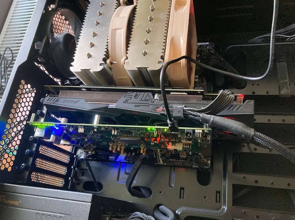
I have one notice about this. Connection is weak and FPGA has no mounting mechanism. For example, competitor Kintex KC705 eval board on all photos have standard bracket for mounting. PolarFire Evaluation Kit has nothing like this and board wobble in the long PCIe slot.
For reason mentioned in previous section I decided to use extension cable from Samtec. I received it for free Samtec as a Free Sample. I would like to thank Samtec for it. I was curious if cable affect performance somehow, but opposite was true. FPGA and data transmissions worked like a charm and allowed me easily to play with FPGA (switches buttons, jumpers, debug pinheads, …) on the desk outside computer. Because FPGA has no mechanical mounting mechanism, I recommend using it in this way. Note that Microchip documentation related to PCIe demo also mention using FPGA connected by similar (maybe the same?) cable to the computer.
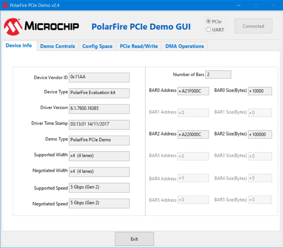
After connecting board FPGA to the PC and installing driver you can use program provided by Microsemi to evaluate PCIe connectivity bandwidth. After opening you can select if you want to connect to FPGA using PCIe or UART. PCIe option allows you to use more features. UART option needs to connect USB cable to the board. After connecting first tab shows details about device and driver. It also shows configuration of BAR. BAR is mechanism of mapping memory of PCIe device to memory space. It is more complicated because x86 have two address space (standard memory and 16-bit Input/Output space). FPGA mapped to memory space.
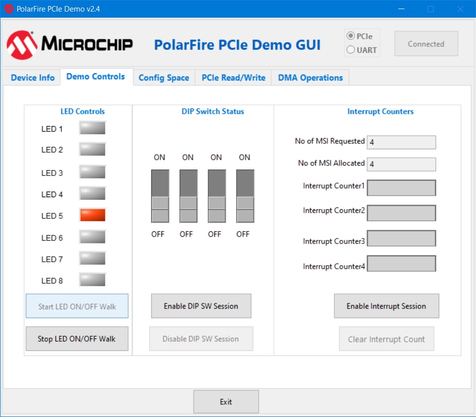
On demo controls tab you can start LED blinking program and read status of some onboard switches.
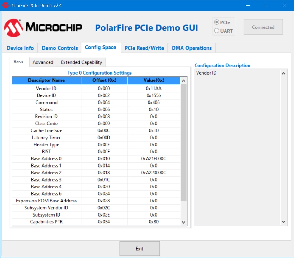
On Config Space tab you can see internal registers of PCIe controller from FPGA. You may note that there many values similar to information shown on Device Info page. At first page they were collected from driver and here they are read from FPGA.
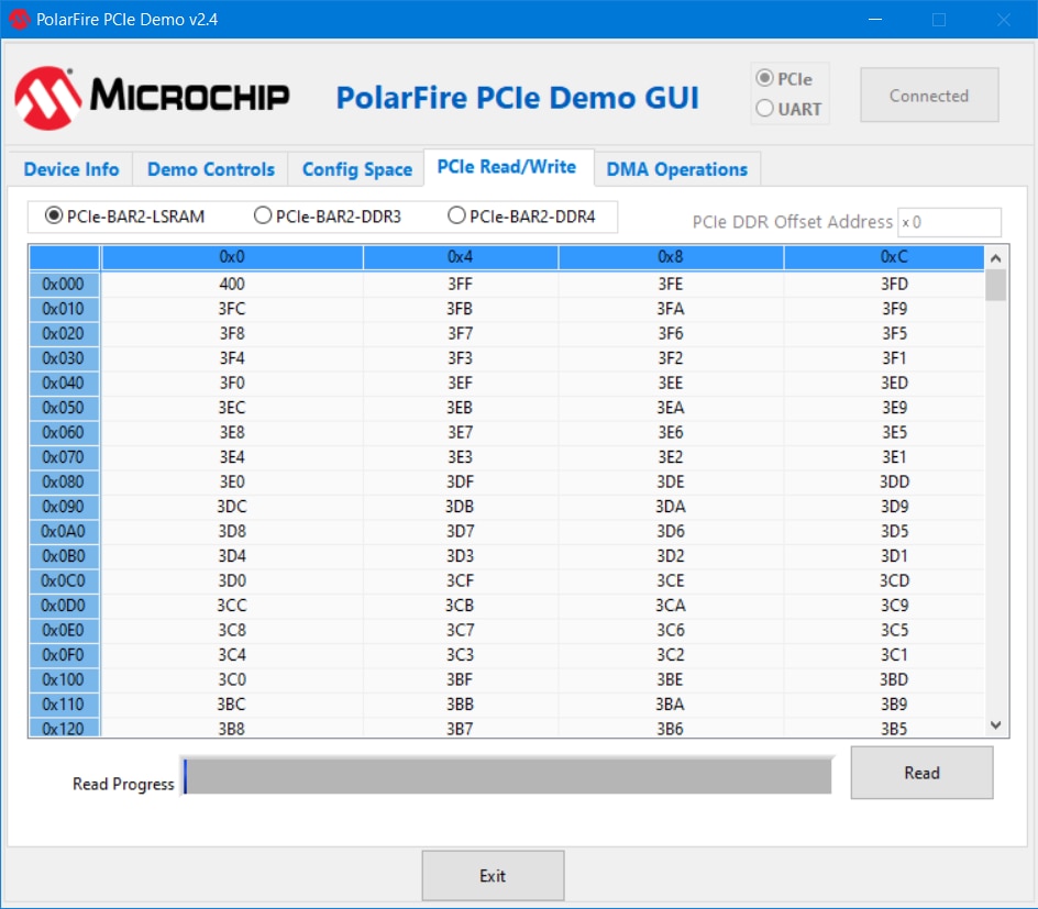
Forth tab you can use for reading and writing memory of FPGA and viewing its data.
Last tab is used for benchmarking. There are three modes including mode when data are transferred directly on FPGA and do not go to or from computer. In all cases you can select direction of transfer, type of memory used on FPGA side, size of transferred data and number of transfers.
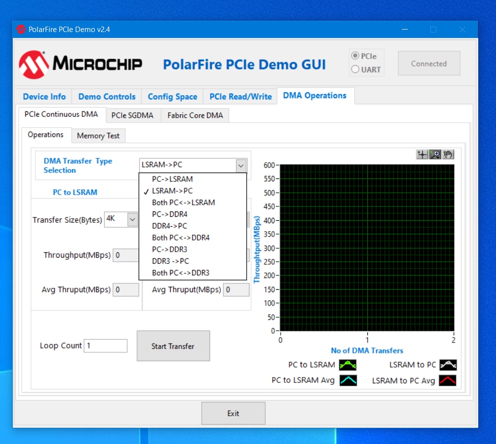
After executing benchmark, you will see Speed of last test, average speed and plot. For example, when transferring 64K of data between PC and FPGA on-chip RAM I received following results. As you can see when transferring data from PC to FPGA is less stable than in opposite direction, but this is natural on non-deterministic computer which runs multiple other tasks.
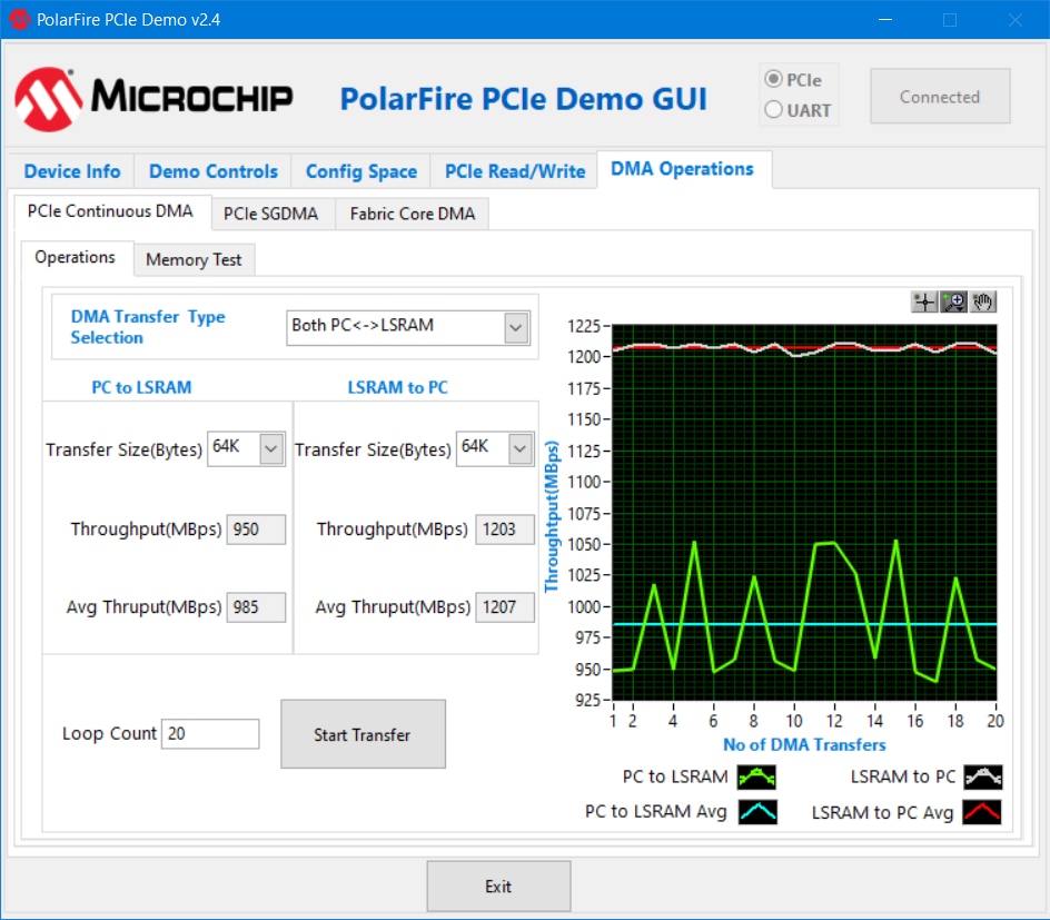
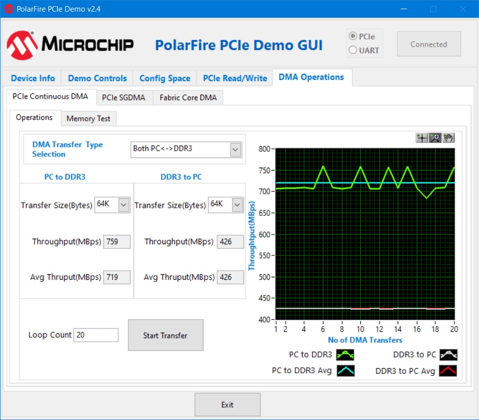
I tried several configs. The on-chip was LPSRAM always the fastest. Except LPSRAM there are two types of DDR memories which are external to the FPGA, and both are installed on PolarFire FPGA Evaluation Board. In case of DDR, memories writes were slower than reads (in case of LPSRAM results were opposite). DDR4 is generally faster. Here is result from the slowest test which I ran with DDR3:
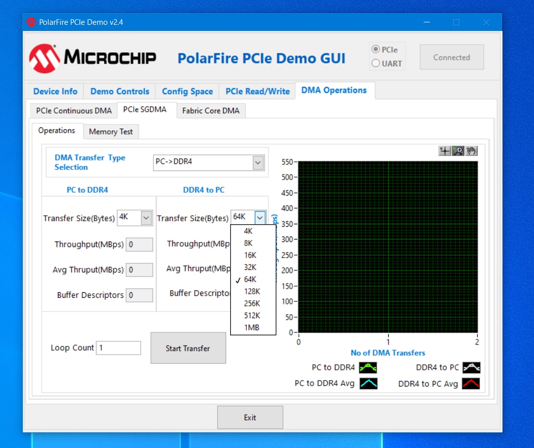
PCIE SGDMA mode support additional and bigger transfers but generally performance was similar to standard DMA.
The last mode transfers data between memories of FPGA. The fastest results I of course achieved when transferring between local memory and DDR4:
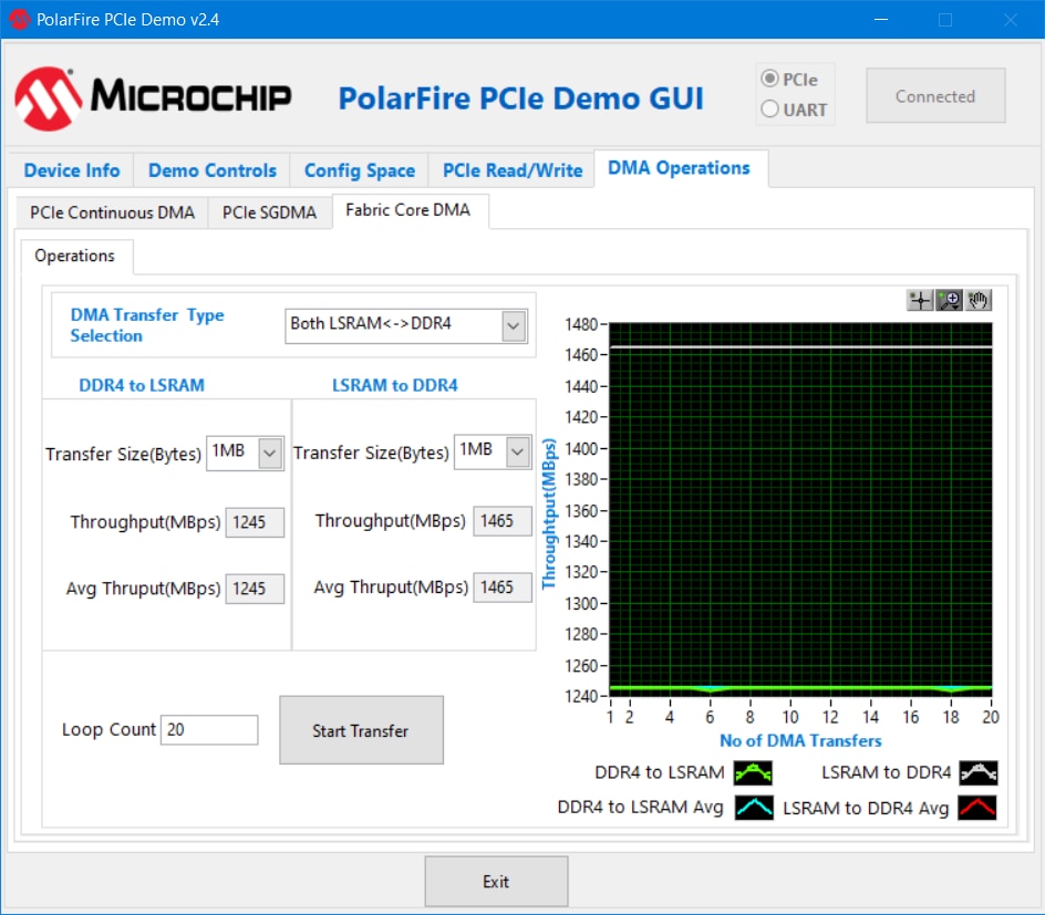
These tests show great performance of FPGA and something like upper boundary on transfer power. You can for example make estimations how much data you can transfer and process when using FPGA in some high-performance server for HW accelerated tasks. Values over 1 GB per second are fantastic and sufficient for almost every task implemented on this FPGA, I think. At these speeds you will most probably reach some other limits.
I originally want to test power consumption as part of experiments with Flash & Freeze but because Flash & Freeze was removed from all documents and demos, then I decided to show power consumption metering with PCIe demo. PolarFire FPGA Evaluation Kit has onboard secondary FPGA which is responsible for power consumption measurements. Microchip provides GUI tool for showing power consumption outputs. It looks as follows when running PCIe demo:
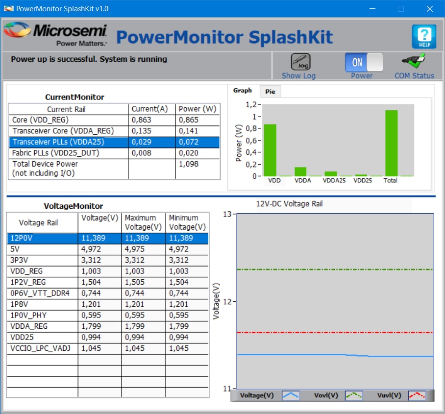
I originally thought that when I start benchmark power consumption will grow but I did not notice this. PCIe demo always consumed about 1 W.
The utility is very minimalistic, I think. It shows bar graph of power consumption on all power branches (possibly it can show it as a pie) and line chart with voltages which can be used for checking voltage drops and so on. If I take that there are big, dedicated FPGA I expected much more detailed outputs and expected for example line charts of currents with high resolution but nothing like this is here. Also note that outputs from this secondary FPGA are send to computer over UART which makes bottleneck on possible data transferred to the PC. I think there is big potential for improvements and new features. But of course, for brief overview of real power consumption of design it is sufficient.
And this is all from my review. I would like to thank again Element14 and Microchip for opportunity to play with this super-power evaluation board of fantastic FPGA. While I was unable to play with Ethernet due to paid licenses, I still enjoyed testing other parts of FPGA even it took me lot of my free time. As part of this review, I learnt using PolarFire FPGA and Libero SoC IDE which I was suing for a first time. I am very satisfied with this board and for this reason I am giving high score in almost all categories.