


As this is the first time I write on these pages, let me shortly introduce myself:
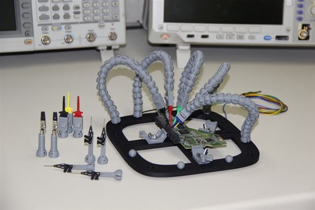
My name is Giuseppe Finizia, I'm an electronic engineer and I work in the Scientific Investigations Department of the Carabinieri (italian police). In particular, I am the senior analyst of the Electronic Forensics Unit of Carabinieri and I deal with technical investigations on seized electronic devices. So I spend almost all the day in a well equipped electronic laboratory. However, very often I felt the need of a tool on which I could place a printed circuit board to perform technical assessments, such as acquire data from a circuit memory, or analyze an I2C or SPI communication bus using a logic state analyzer, and much more. In all these cases, until now I had to use the usual "third hand" tool, but then I decided to create a specific tool for my needs. So I designed this "PCB Workstation with Articulated Arms", with which I can now connect the lab instruments to the individual electronic components to be analyzed.
So, I wish to share with the element14 community this 3D printed project:
http://www.thingiver...om/thing:801279
Although there are many good free 3D modeling software, for this project I used "MOI 3D" (www.moi3d.com) because it is very powerful and easy to use.
Printing all the parts could be a challenging task using a not adeguate 3D printer. I have used my ZORTRAX M200 which is a very accurate and high resolution 3D printer.
Anyway, I have just updated the thingiverse.com page of my project by providing detailed instructions for 3D printing, so you can get there more details about this benchtop tool.


