


With the promise of new 5G technology on the horizon, there is no doubt that electronics companies are faced with new challenges to meet the demands of the higher performance technology, and it’s a race too. These challenges are being faced by test and measurement companies, integrated circuit design companies, as well as PCB and interconnect companies. The trouble stems from the high frequencies 5G needs to operate at, to provide the speed and low latency it has promised.
The frequencies associated with 5G technology can be split into two general categories, below 6GHz and above 6GHz. Currently, frequencies below 6GHz are used for a vast majority of wireless communications and are familiar to many designers. On the other hand, frequencies above 6GHz, have been previously inaccessible to engineers due to technology limitations. Such frequencies include 28GHz and 39GHz.
Due to the laws of physics, certain limitations are encountered when working with the high frequencies associated with 5G technologies. Generally, signal loss is much greater for all mediums of signal transmission. This includes free space (over the air), PCB routes, interconnects, and cables. While we are basically stuck with the loss of free space signal propagation, improvements have been made to other mediums to help measure and test higher frequency circuits as well as detect and condition higher frequency signals for use in final applications.
Interconnects in systems can sometimes be taken for granted. However, they are just as important as the rest of the pieces in a system. If the interconnect fails, the system will fail. An example of an interconnect designed specifically to handle the higher frequencies of 5G systems is the solderless end launch connector. These are available from companies such as Amphenol, Samtec, and Southwest Microwave. In addition, they come in various sizes that support different frequency ranges. Generally speaking, the smaller the connector size the higher the frequency it supports. 3.5mm connectors are usable to 27 – 34GHz, 2.92mm connectors operate to 40GHz, 2.4mm connectors are usable to 50GHz, while even higher frequency applications can use 1.85mm and 1.0mm connectors that extend operating frequencies 67GHz and 110GHz respectively.
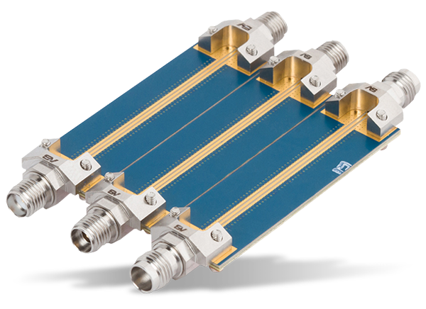
Figure 1. Amphenol solderless PCB edge launch connectors: (Image credit Amphenol)
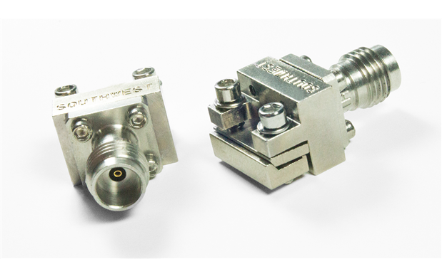
Figure 2. 1.85mm Southwest Connector front and side view: (Image credit Southwest Microwave)
The solderless connectors feature a pin that rests on the PCB trace when connected. This pin-to-PCB interface is what provides the electrical connection for the signal path. However, the pin adds a small amount of capacitance to the transmission line when mounted which will create a small discontinuity in the signal path. If soldered, additional capacitance is added, that is undesirable. Therefore, for the best performance, the signal transition path from the connector pin to the PCB trace should be left unsoldered. The vendors also offer the connectors with various pin diameters. The correct diameter depends on the PCB used in the application. Thinner dielectrics result in a more narrow 50 Ohm transmission line. On the other hand, thicker dielectrics will yield a larger 50 Ohm width. Therefore, for best performance from the connectors the PCB technology used should be taken into consideration.
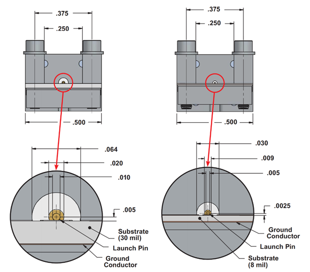
Figure 3. Image showing different pin diameters used on two different sized substrates (Image credit: Southwest Microwave)
Studies have also been done to find methods of reducing the discontinuity presented from the pin to PCB transition. These include adding small tapers to the end of the PCB trace where it meets the connector. The taper adds a small amount of inductance that cancels out the parasitic capacitance leaving a more constant 50 Ohm transition impedance. It is possible to over compensate for the capacitance, and the taper geometry will vary based on the dielectric thickness and properties. Therefore, the best result is obtained through simulation and optimization.
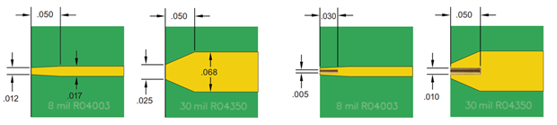
Figure 4. Example Tapers: (Image credit:http://https//mpd.southwestmicrowave.com/wp-content/uploads/2018/07/The-Design-and-Test-of-Broadband-Launches-up-to-50-GHz-on-Thin-and-Thick-Substrates.pdfSouthwest Microwave)
Although tapering the end of the route may seem a bit excessive, it can be shown that even a miniscule amount of parasitic capacitance can add a decent amount of loss and discontinuities to the transmission path. For example, a parasitic 0.1pF of shunt capacitance is negligible at frequencies such as 2.4GHz and 5.8GHz. On the other hand, when working at 5G frequencies such as 28GHz and 39GHz, the insertion loss can exceed one dB. Furthermore, the return loss becomes much worse. This can create undesired signal reflections and discontinuities in the signal path. This can further be seen in the plot shown below.
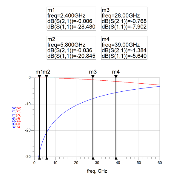
Figure 5. S-Parameters plot showing insertion loss and return loss due to 0.1pF of parasitic capacitance (Image credit: ME)
In addition to the end/edge launch connectors discussed above, solderless connectors are also available in surface mount versions. The surface mount connectors are available with two different pin connections styles. Both feature a small pin which extrudes just enough from the housing to make contact with a signal trace. The first is designed to be used with microstrip and coplanar wave guide (CPW) routes. It has a “mouse bite” feature which allows the signal path to route out of the connector housing unobstructed. The second style is designed to be used with stripline or buried routes. This is meant to make connection with a plated via to carry the signal to the inner PCB layers.
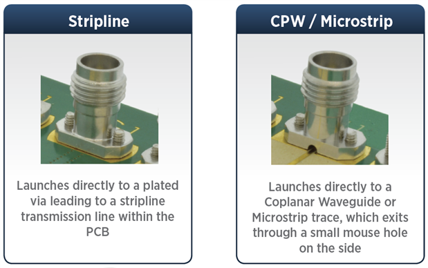
Figure 6. Two of the surface mount connectors available (Image credit: Avnet)
The testing of components and systems is a critical part of engineering. Circuits must be validated, optimized, and tuned to get the absolute best performance in their final application. As a result, care and consideration are needed when creating a test setup. A bad connector or cable can make circuits appear to perform worse than they really are and provide inconsistent results. This can lead to extended test time and frustration.
Overall, system performance and system testing can greatly benefit from a carefully designed interconnect. Choosing the proper connector for an application demands careful consideration and in some cases, simulation to assist in the design choice. However, with the many choices now available for 5G interconnect solutions, the best solution can more easily be obtained.
Have a story tip? Message me at: cabe(at)element14(dot)com
