Table of Contents
- Introduction
- Renesas RA4M1 Overview
- Evaluation Board Overview
- Pre-Loaded Demo
- Software Installation
- Building an Example Project
- Uploading and Running Code
- Creating a New Project
- Adding GPIO to the Project
- Adding a DAC to the Project
- Adding a Timer to the Project
- Adding USB Serial to the Project
- Putting it All Together: A Configurable Ramp Generator
- Summary
Introduction
The Renesas RA series of microcontrollers looked interesting, so I decided to try out a development/evaluation kit! I went for the RA4 series, which is intended to be midrange. More specifically, I went for RA4M1; the M means it is the mainstream/low-power range. Incidentally, the new Arduino Uno R4 also uses RA4M1.
The RA4M1 contains a Cortex-M4 core, a decent amount of storage, 14-bit ADCs, 12-bit DAC, USB, CAN, LCD support, and a variety of other features, so it is fairly versatile! It’s also easy to solder with QFP and QFN packages available. Renesas microcontrollers have excellent documentation, so I had high hopes. I was expecting it to be a pleasure to try to use this device, and you can judge for yourself by reading on, but from my perspective, it didn’t disappoint.
This blog post covers the following things:
- Brief description of the chip and the development kit
- Compiling a demo project
- Creating a new C project from scratch
- Adding peripherals, namely GPIO, DAC, Timer and USB Serial
- How to locate information on each peripheral in the SDK documentation
The blog post ends with a simple project that combines all these peripherals.
After you have finished with this blog, if you're still interested in exploring the RA4M1 further, possibly you may be interested in the following blogs too:
Using Segment LCD and ADC with Renesas RA Microcontrollers
Adding a Dual Number Display Segment LCD to Renesas RA Microcontrollers
Pulse Width Modulation (PWM) with Renesas RA series Microcontrollers
Click here for all blog posts tagged RA4M1.

Renesas RA4M1 Overview
The Renesas RA family contains Cortex-M4, -M23 and -M33 cores. The RA4M1 contains a Cortex-M4 core.
The EK-RA4M1 development board contains a RA4M1 chip with product code R7FA4M1AB3CFP , which is the 100-pin QFP version. There are 64, 48 and 40 pin options in various easy-to-use surface-mount packages too.
The RA4M1 chips all contain 246kbytes of Flash, plus an additional 8kbytes of “Data Flash”, and 32kbytes of RAM. The chips operate over a large voltage range: 1.6 to 5.5V. All have several 16-bit and 32-bit timers, as well as several 14-bit ADCs (with conversion times under 1us), and a 12-bit DAC (30us conversion time). They all have a CAN interface, support 12Mbit/sec USB host or peripheral, support lots of capacitive touch inputs, and can even drive multiplexed LCD screens. The 100-pin QFP chip even contains four op-amps, and four UARTs!
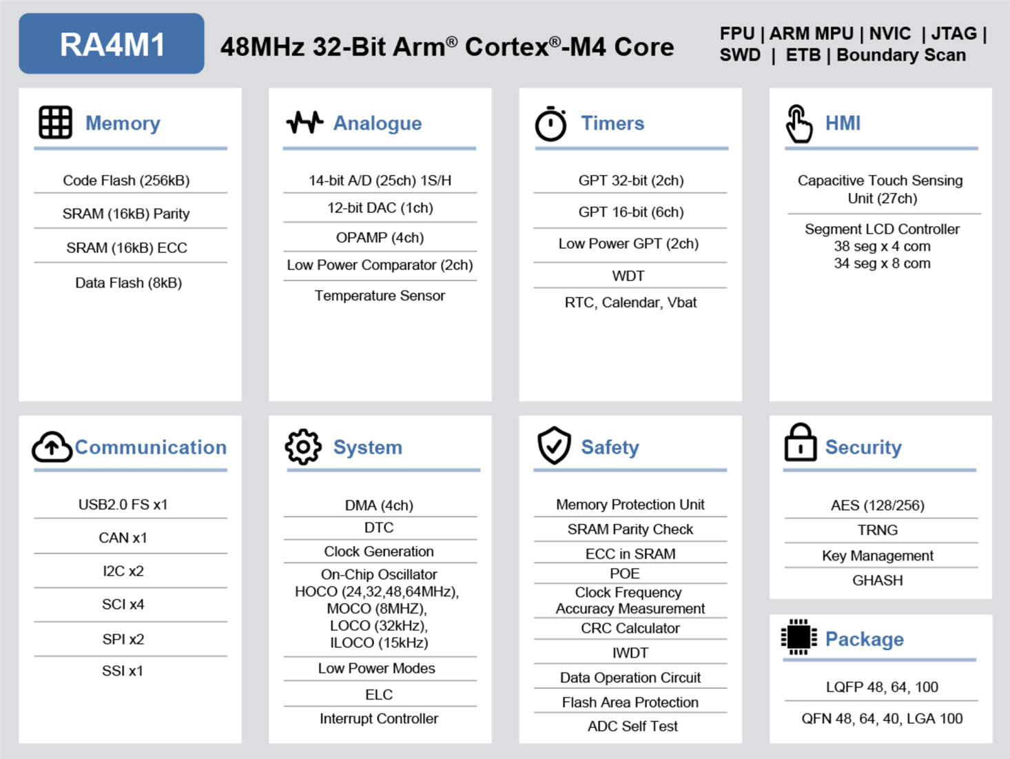
Typical current consumption can reach around 18mA at 48MHz with all peripheral clocks enabled. At 1 MHz the figure is 1mA. At 32.768kHz it is 8.5uA. With the peripheral clocks disabled, the current drops to 5uA. In standby modes the typical value is 0.8uA (4.5uA max) at room temperature. The RTC can continue to run when the microcontroller is off; it consumes 0.8uA typical.
Evaluation Board Overview
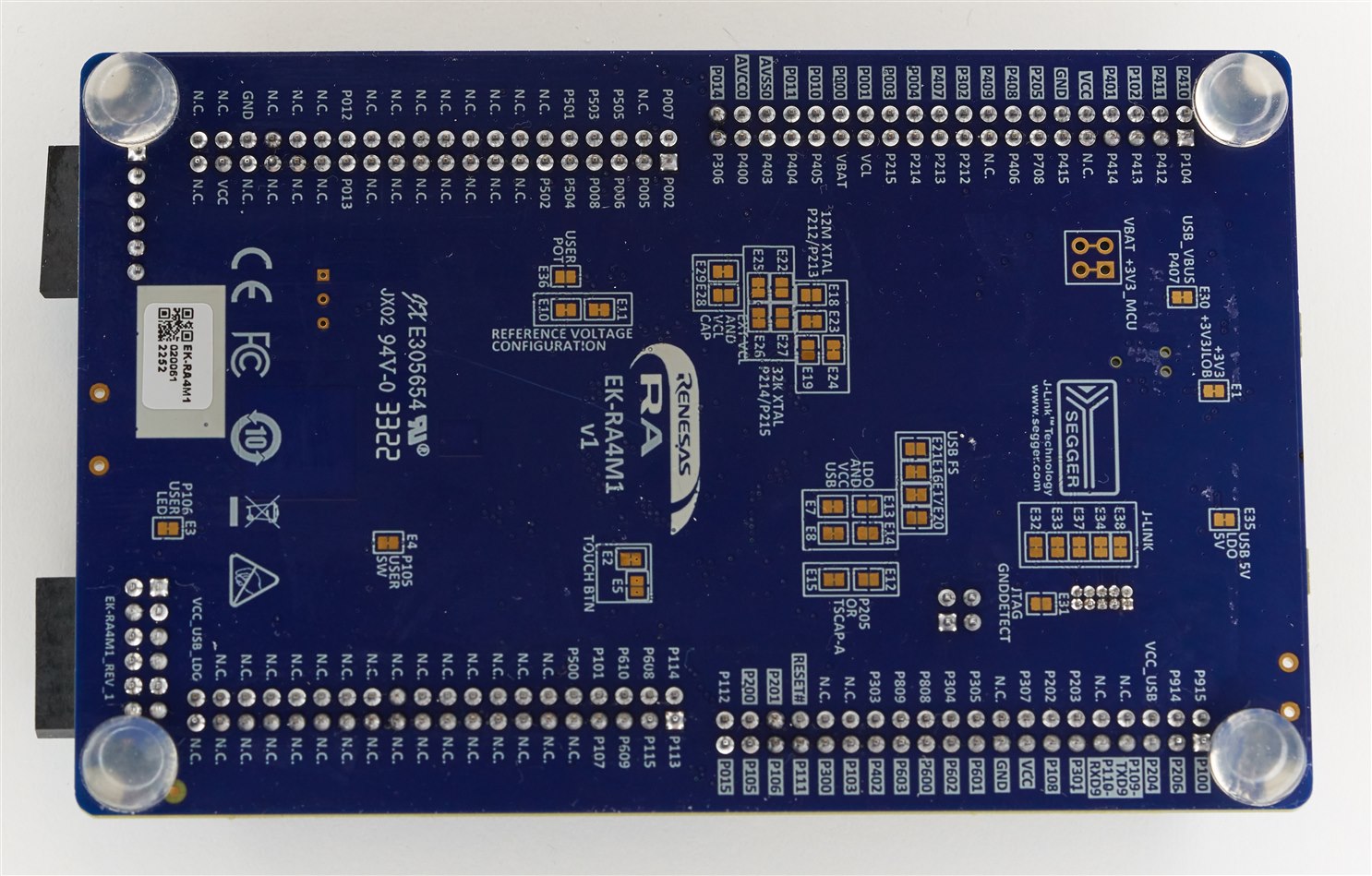
The evaluation board, EK-RA4M1 , is quite large, with pin header access to everything. There are also a couple of PMOD connectors. I like that the board brings out a USB connection to the on-board J-Link debugger (which is used to upload built code to the microcontroller and perform step-by-step debugging) but also brings out a separate connection for the USB interface on the RA4M1 microcontroller too.
I didn't like that the header pin labels on the board are tiny - a magnifier is needed! Also, the GPIOs are mapped to header pins in no logical sequence; it seems random. It would have been nice to see the connections grouped by port numbers.
To use the board, power is applied to the USB connector labeled Debug. The other USB connector won’t do anything unless the application's code on the RA4M1 chip assigns it to a purpose. The pre-loaded demo implements a USB serial interface for displaying a menu over that USB connection.
There are not many external peripherals on-board; just a button, LED, and a touch sensor pad.

The underside of the board has many shorted pads, which could be cut if signals need to be isolated.
Pre-Loaded Demo
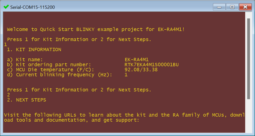
The pre-loaded demo on the board doesn’t do much, but it does demonstrate the USB interface on the RA4M1, providing USB Serial device functionality.
To run the demo, I connected two micro USB cables (one very short cable is supplied, but you’ll need a second cable) to the PC. One connects the PC to the debugger (and also provides power to the board), and the other connects the PC to the USB interface on the RA4M1 chip. A simple menu appears when Enter is pressed in the serial terminal (e.g. PuTTY).
Software Installation
Working with the RA4M1 requires the download of Renesas’ Flexible Software Package (FSP) - the package contains the Eclipse-based development environment (called e2 studio) and FSP, all bundled in one.
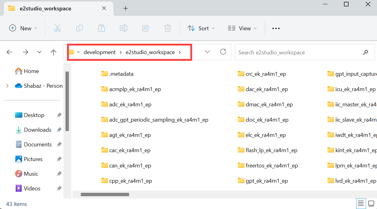
When e2 studio is run, it will prompt for a workspace. I created a sub-folder in a development folder and typed that path, for instance:
C:\development\e2studio_workspace
Next, I clicked on Import sample projects, selected the R7FA4M1AB device, and then selected the EK-RA4M1 Example Project Bundle (it contains many examples).

After that is installed, you’ll see a load of project folders in your workspace using Windows Explorer:
In e2 studio, the Project Explorer can be displayed (if it is not already visible) by selecting Window->Show View->Project Explorer.
All the projects are actually open, so they should be closed. Click anywhere in the Project Explorer, press Ctrl-A to select all, then right-click and select Close Projects.
In future you can open just a single desired project by selecting the single project, right-clicking, and selecting Open Project.
Building an Example Project
I opened the quickstart_ek_ra4m1_ep project from the Project Explorer, as shown here:

I edited the code to print a custom message within the menu. The modified file was called src/hal_entry.c - this file contains a hal_entry function which is effectively where user code execution begins after the C environment is started up. You won't be writing code in a traditional main() function because the auto-generated main function calls hal_entry().
Note that you cannot just click the hammer icon and let the code build., because the first step is configuring the project. To do that, double-click on configuration.xml in the Project Explorer and wait for a configuration view to display in the main pane. It will be in a Summary tab, but there are other tabs to explore too. Click on Generate Project Content. Some information briefly appears in the status bar at the lower-right of e2 studio, but other than that, it’s easy to miss that the Generate Project Content button has done anything, but it has! Typically, it will create auto-generated code in the ra_gen folder.

Now you can click on the hammer icon and the code will build.
Uploading and Running Code
Click on the bug icon, and eventually, a J-Link Firmware Update window may appear the first time. Click on Yes. Afterward, once the firmware is updated, you may need to press the bug icon again.
Setting up a Debug Configuration
Note that if you press the bug icon and get a message as shown in the screenshot below, you’re probably running a new project and have not set up any ‘debug configurations’ yet. If you don’t get any error messages, skip to the next section.

Click on the small black triangle next to the bug icon, and select Debug Configurations. Right-click on Renesas GDB Hardware Debugging and select New Configuration.

In the window that appears, click on Configure Workspace Settings. Close the window, and then see if a default Debug Configuration has been created. I think there’s a bug, because you should not need to do this. I only encountered this problem on my first project, and subsequently, I always saw a <project_name>_Debug_Flat configuration for future projects.
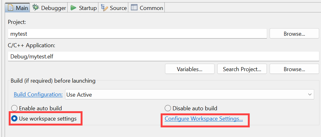
If this doesn’t work, you may need to configure the tabs in the screenshot above manually. In that case, in the Debugger tab, select J-Link ARM and select R7FA4M1AB for the target device. I didn’t need to do this manually.
Running a Debug Configuration
Click on the bug icon. When the Eclipse view changes to the Debug Perspective, you can click on the green triangle to run the code. Press the green triangle a second time if the code immediately stops because the Debug Configuration has been set to automatically insert a breakpoint at the main() function (you could remove that from the configuration if desired).
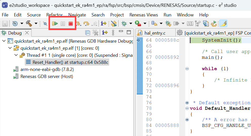
You should see the red LED blinking on the development board because that is what this code is supposed to do. Use a serial terminal (such as PuTTY) and press Enter to see the modified message appear, which proves that the modified code was successfully built and uploaded to the board.

Press the red stop button, and then switch back to the C/C++ code view by clicking on the C/C++ perspective button near the top-right of e2 studio.
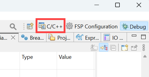
Note that the code is permanently in Flash memory. If you disconnect the USB power/debugger cable and reconnect, or if you press the Reset button on the board, the code will automatically run.
Creating a New Project
Click on Help->Welcome and then select Create a new C/C++ project.
Select Renesas RA.
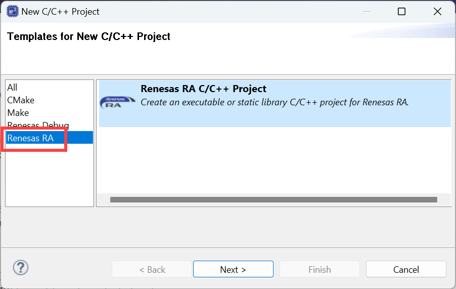
Select the correct part code and the latest toolchain (if you have more than one toolchain installed on your PC). Select C++ if that’s what you prefer.
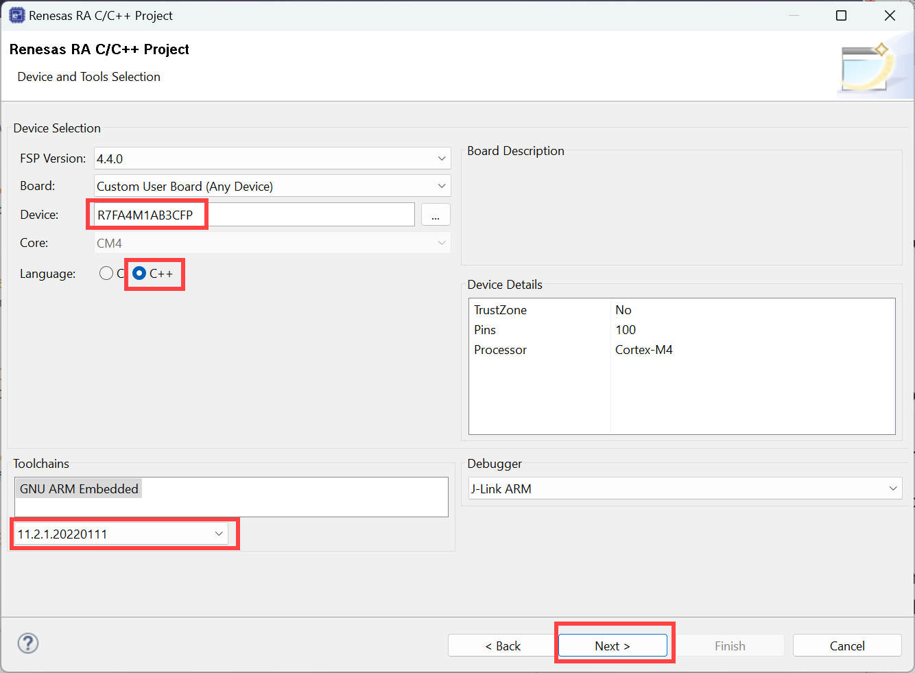
The project will be created, and you can click on the hammer icon to build it successfully, although the project currently does nothing.
Adding GPIO to the Project
Double-click on configuration.xml in the Project Explorer, and then click on the FSP Configuration view to expand it. There are tabs labeled Summary, BSP, Clocks, Pins, etc. Select the Pins tab, and then choose the pin to modify. Since the development board has an LED connected to P106, I expanded port P1 and selected P106, and then set the mode to Output, and the Drive Capability to Medium. Click Save, and then click Generate Project Content.
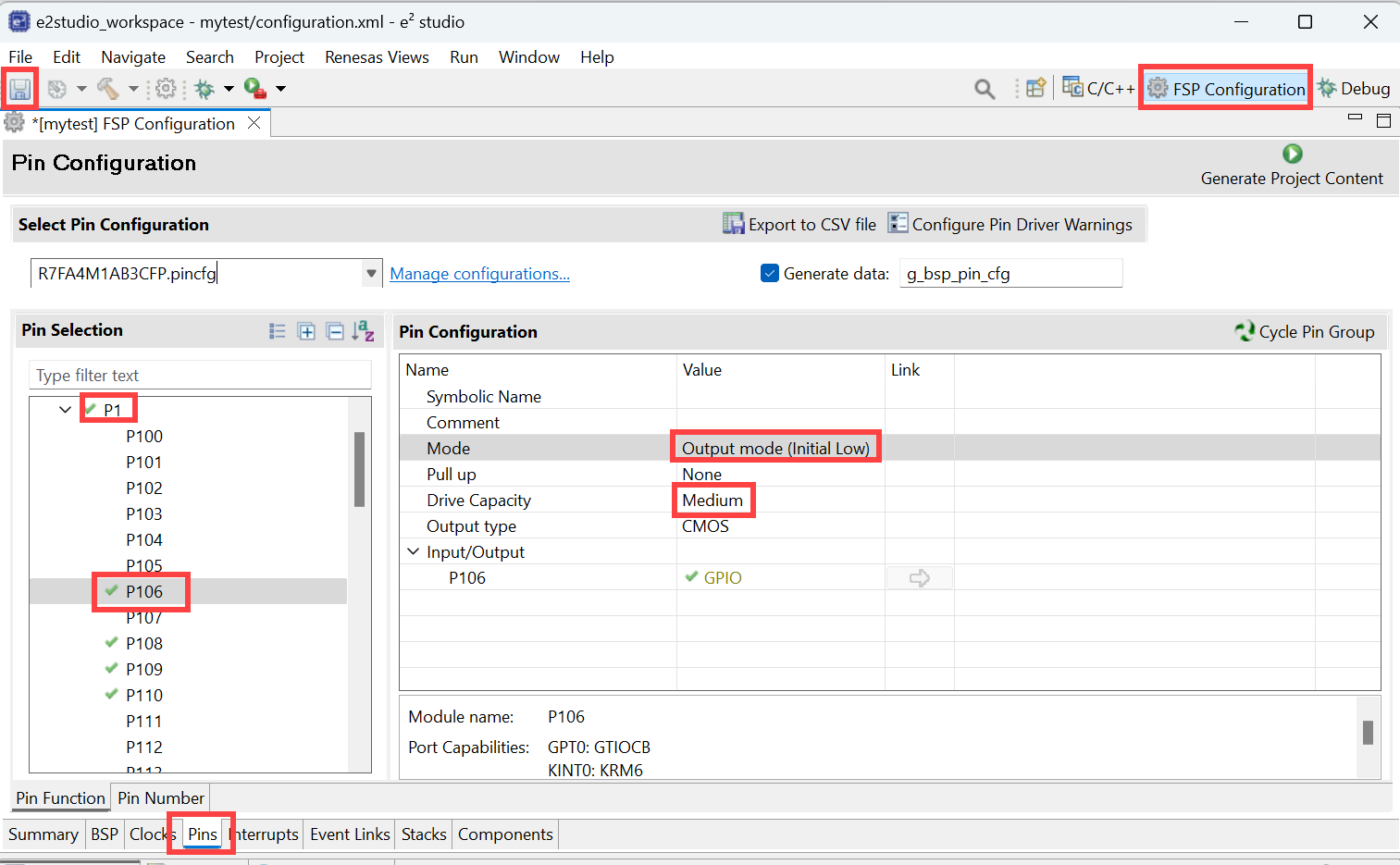
If you click on the Stacks tab, you’ll see the following:
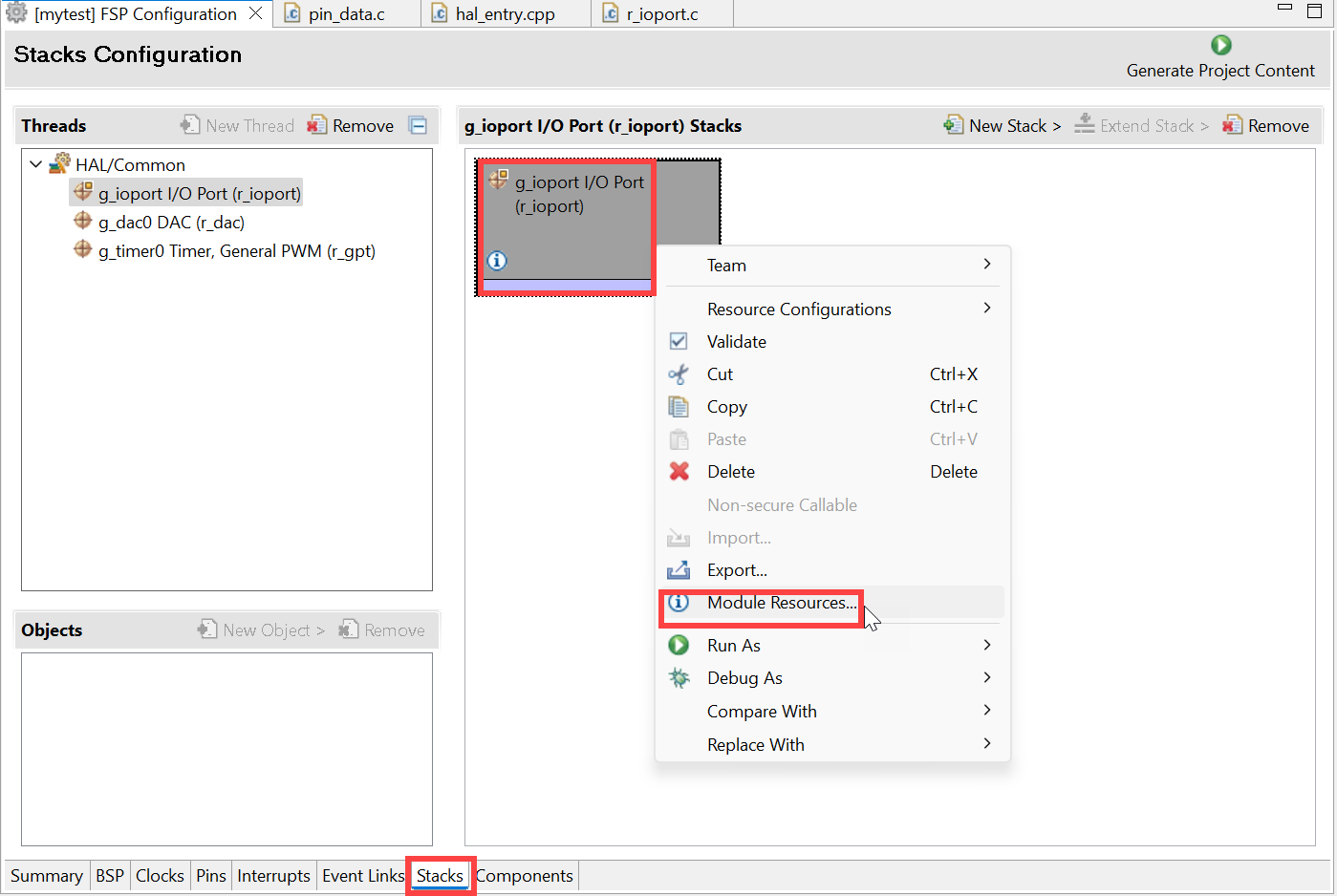
Selecting the g_ioport (r_ioport) box that is there and right-clicking, and then clicking on Module Resources, as shown in the screenshot above, will open up web documentation that explains it. Scrolling down that web page provides the example code to control GPIO.

Another way of getting to that documentation is to simply go to the Renesas FSP web documentation link and then, in the search box at the right side, type r_ioport (r_ioport was displayed in the box in the Stacks tab screenshot earlier) and press Enter.

Again, you’ll find the same example code if you scroll down at that page.
Here is how the pin can be turned on to illuminate the LED on the board:
#define LED_PIN BSP_IO_PORT_01_PIN_06R_IOPORT_PinWrite(&g_ioport_ctrl, LED_PIN, BSP_IO_LEVEL_HIGH);
A working example of this is shown further below in the Putting it All Together section to blink the LED.
Adding a DAC to the Project
The DAC pin can be configured using the FSP Configuration’s Pins tab:
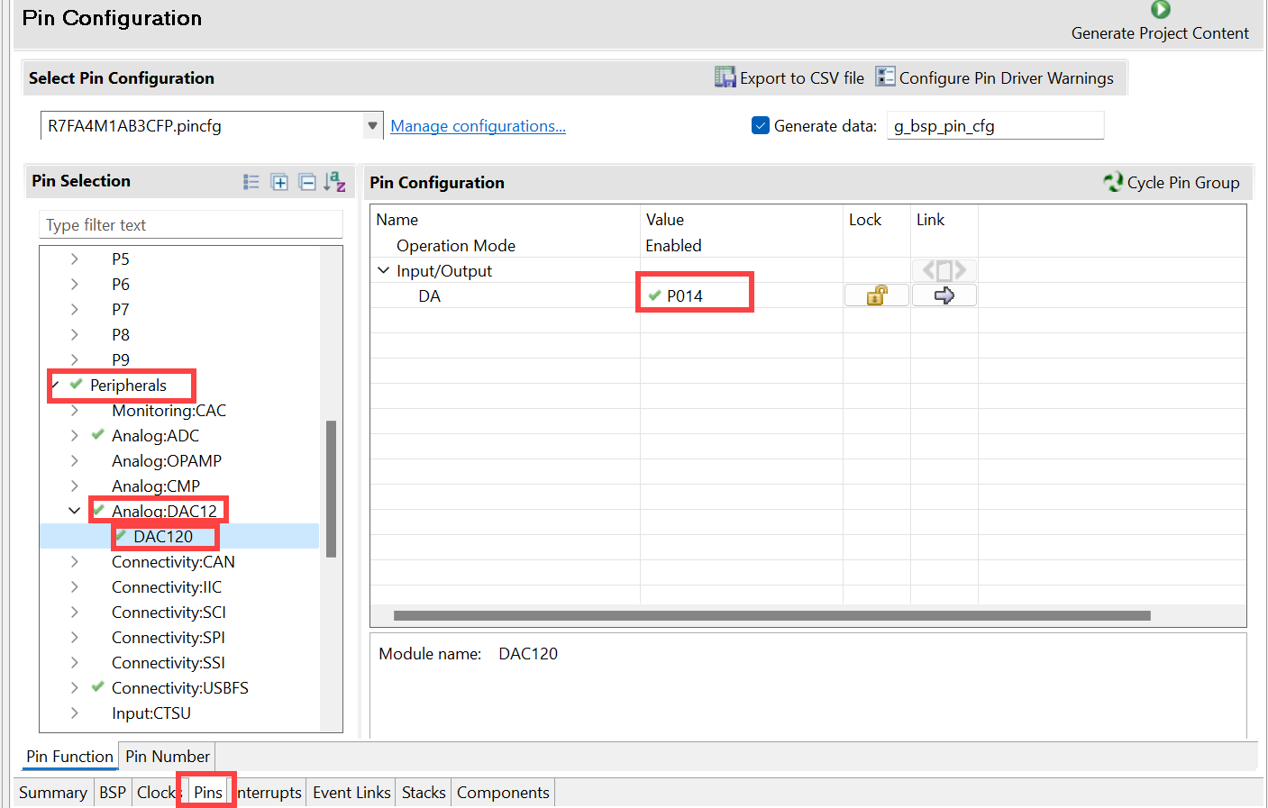
The FSP Configuration’s Stacks tab is used to add drivers.
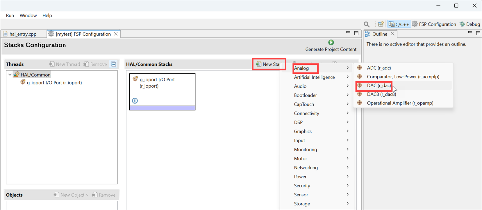
Once you do that, click on the box in the HAL/Common Stacks pane, and then the tab for Properties for it can be selected below. Ensure that the pin configured in the Pins tab is visible, as shown in the screenshot below.
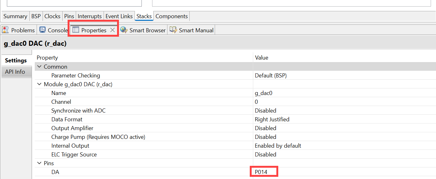
Save the configuration and click on Generate Code.
The easiest way to find out how to use the DAC is to navigate to the FSP online documentation and then type DAC in the search box on the right side.

Scroll down, and there’s a nice example.
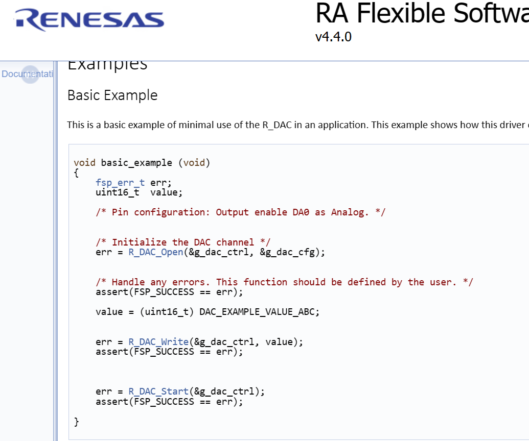
Note that the example uses variables called g_dac_ctrl and g_dac_cfg, but the Properties pane in the screenshot above shows that the assigned name is g_dac0. Therefore the variable names in the example code would need to be modified to g_dac0_ctrl and g_dac0_cfg.
Then, to use the DAC in the code, the following line will enable it:
R_DAC_Open(&g_dac0_ctrl, &g_dac0_cfg);
To write a value v (between 0 and 4095, corresponding to between 0V and 3.3V) to the DAC, use these lines of code:
R_DAC_Write(&g_dac0_ctrl, v);R_DAC_Start(&g_dac0_ctrl);
Adding a Timer to the Project
As before, open up the FSP Configuration by double-clicking on configuration.xml, and go to the Stacks tab to add a driver. To add the driver, click on New Stack->Timers->Timer General PWM(r_gpt)
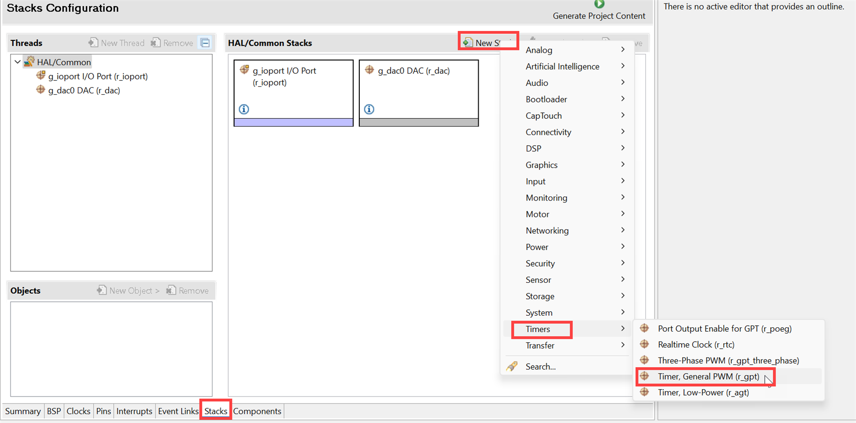
Click on Properties below that, and you’ll see the clock source is PCLKD. The Clocks tab in the FSP Configuration can be used to see what that frequency is (it is 48MHz).
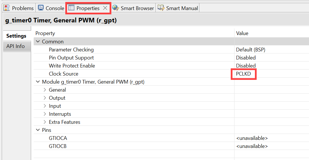
Save the configuration and click on Generate Project Content.
The documentation for the timer can be found by searching for it at https://renesas.github.io/fsp/ as before:
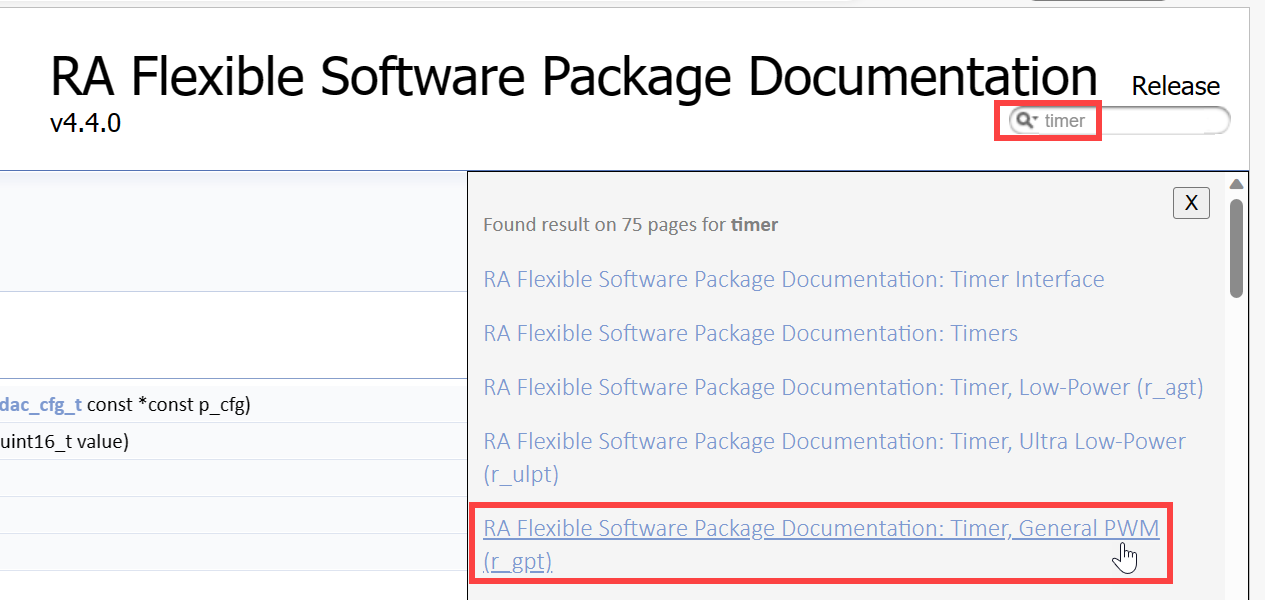
Scroll down to find a suitable example:

So, to configure the timer to continually count upward (and then cycle around), use the following line of code:
R_GPT_Open(&g_timer0_ctrl, &g_timer0_cfg);
Then, to start the timer, use:
R_GPT_Start(&g_timer0_ctrl);
You can also reset the timer (while it continues to run) by using:
R_GPT_Reset(&g_timer0_ctrl);
Adding USB Serial to the Project
USB Serial is extremely useful, since it can be used for printing troubleshooting messages to any connected PC or for displaying user menus and configuring applications.
Adding USB Serial is a little more involved than the other peripherals added to the project so far, but that’s to be expected since USB is more complicated. It’s not too bad, however.
First off, as with other peripherals that have been added, double-click on configuration.xml to open up the FSP Configuration window, and then click on New Stack, and this time click on Connectivity and choose USB PCDC. PCDC refers to Peripheral Communication Device Class. The RA4M1 supports USB host or peripheral mode operation, but perhaps peripheral is the most expected scenario for typical microcontroller projects. CDC provides USB Serial functionality with no drivers required for connected PCs.
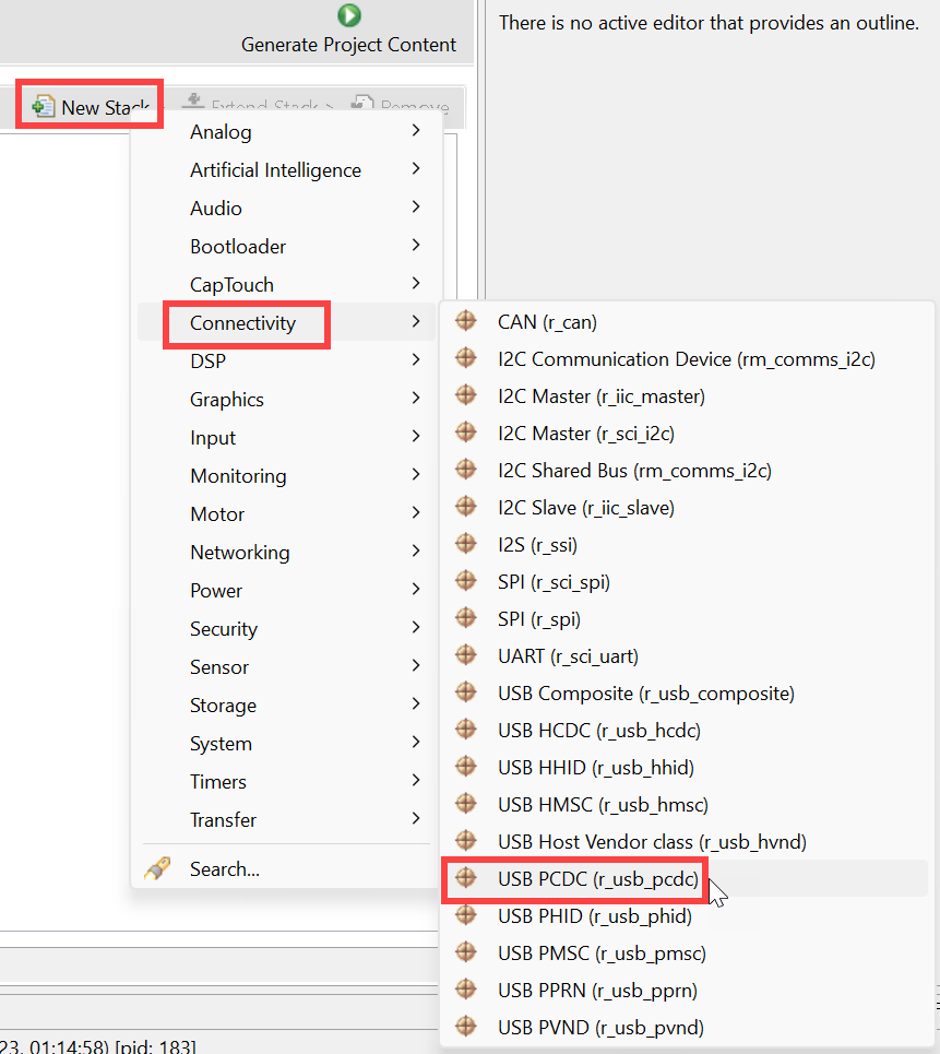
A load of blocks will be displayed in the Stacks pane:
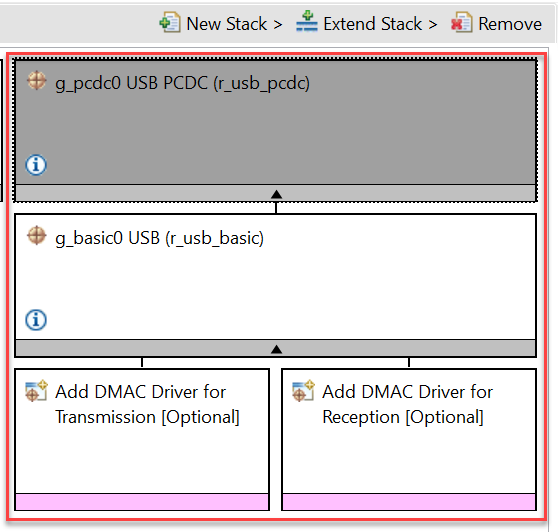
Next, click on the Pins tab, and navigate to the pin selection shown in the screenshot below. Set the Operation Mode to Device, and then the rest will automatically fill with the pin numbering detail. Nothing else needs to be changed once you have modified the Operation Mode.

As before, click Save, and then click Generate Project Content.
The online documentation for USB Peripheral CDC can be found by going to https://renesas.github.io/fsp/ and searching for it, as shown in the screenshot below.

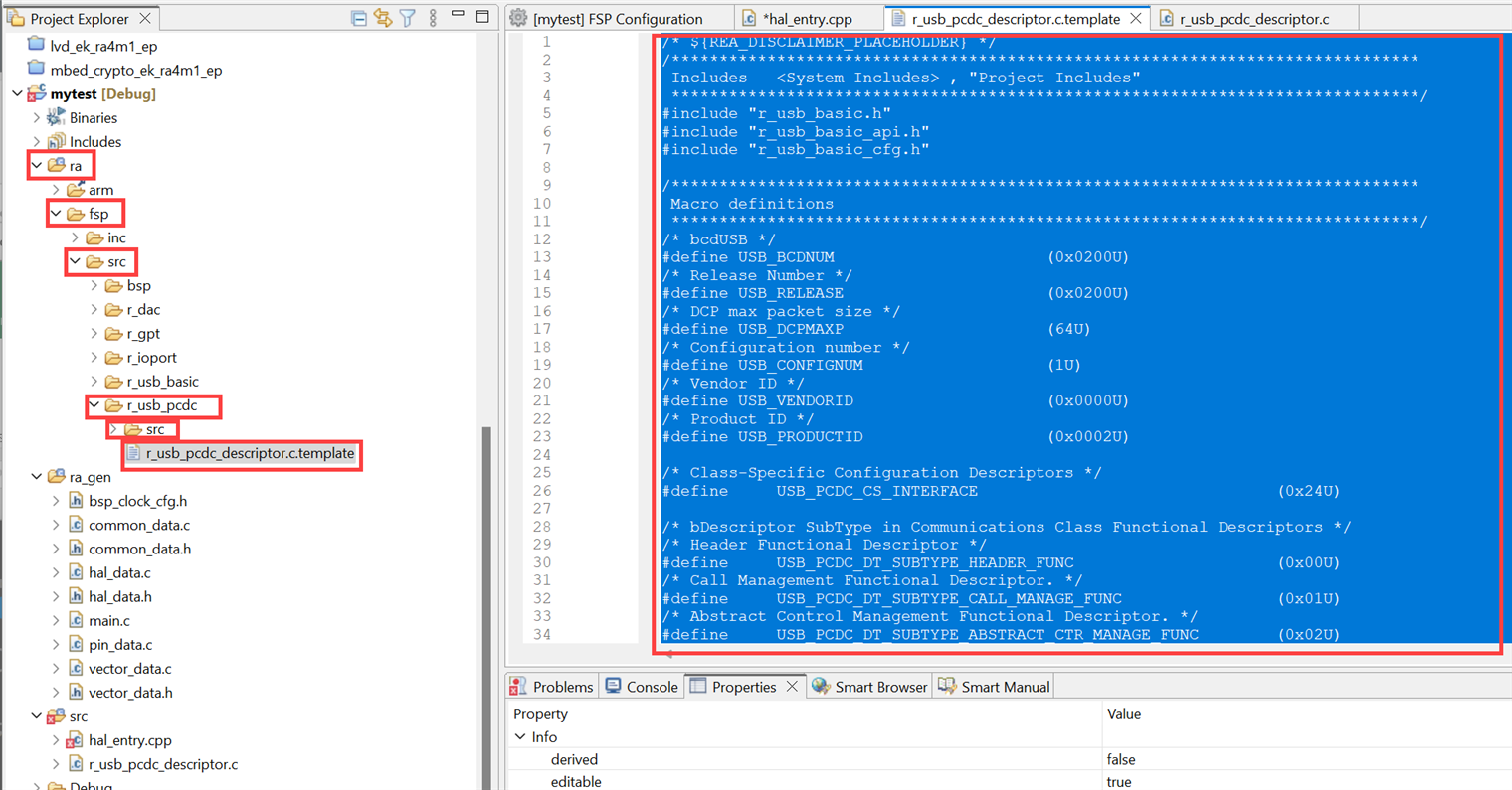
According to that documentation page (scroll down to the end of that page), the code needs to include USB configuration structures, and an example template is supplied in a file called ra/fsp/src/r_usb_pcdc/r_usb_pcdc_descriptor.c.template
Go to that location and copy the content to the clipboard.
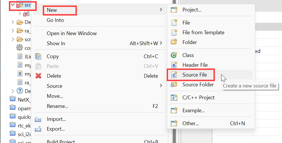
Next, create a new source file in the src folder, by right-clicking on the src folder and selecting New->Source File.
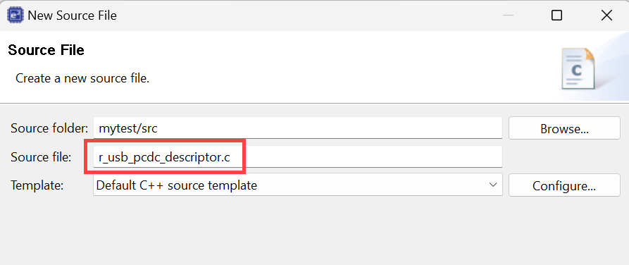
Give the new file the name r_usb_pcdc_descriptor.c
Paste the copied template content into the new file and save it. No other changes need to be made to the file.
The documentation provides some example code; a snippet is shown below. This usb_pcdc_example function basically starts up the USB capability and then continually loops, waiting for any USB event to occur. If any character is typed by the user on the PC’s serial console software (such as PuTTY), then the function will send back that same character to the PC.
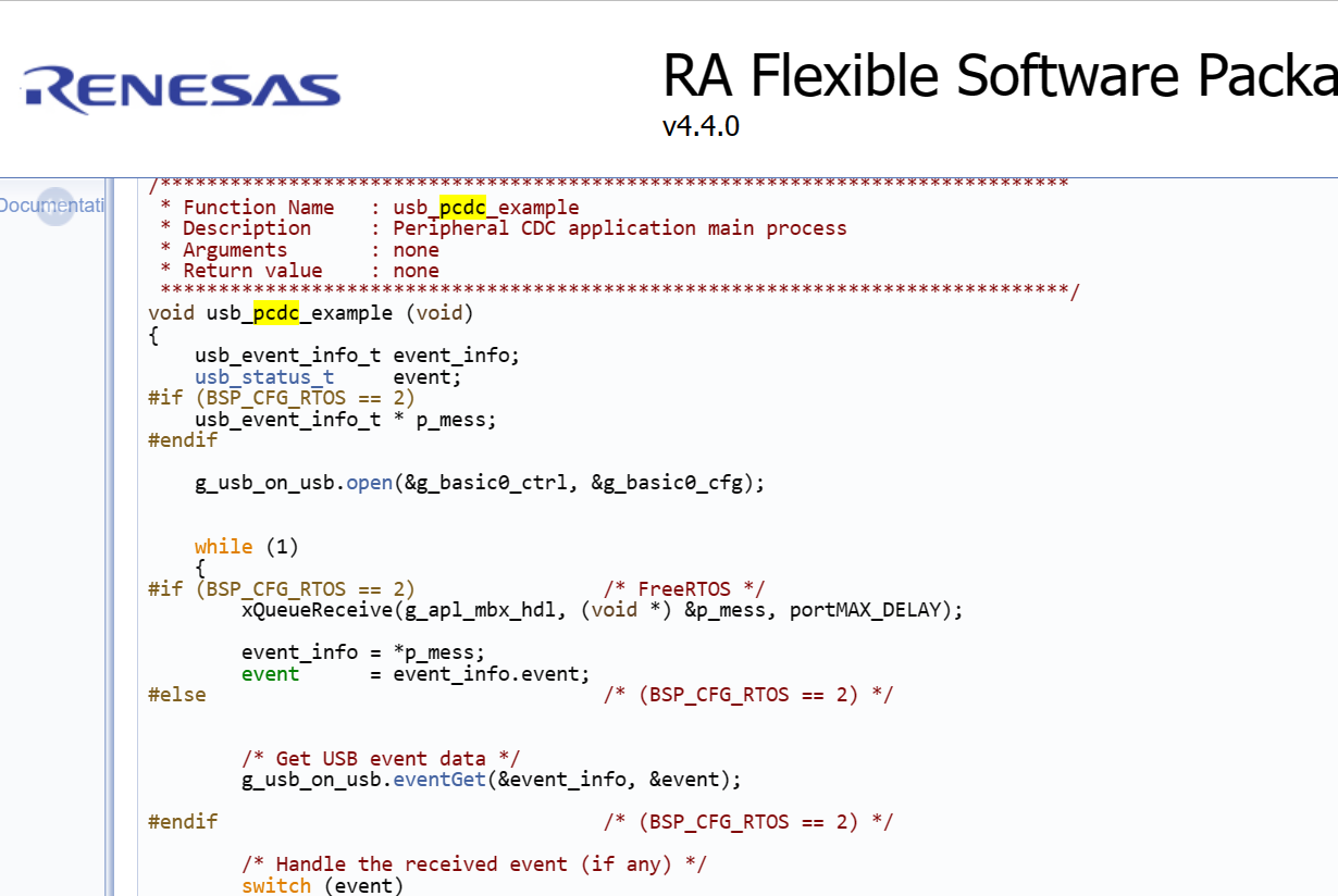
For a more normal use-case, the content in the usb_pcdc_example can be separated into a couple of functions, with the first one opening up the USB capability:
void usb_setup(void) { g_usb_on_usb.open(&g_basic0_ctrl, &g_basic0_cfg);}
The remainder of the code in the usb_pcdc_example function could have the forever while loop removed and the function renamed to (say) usb_poll, and then it could be called from any main program loop repeatedly.
A better solution would be to use a timer and its callback to call usb_poll, but I went for the simple option for now.
Within the usb_pcdc_example function, it is possible to see how data is read and written over the USB serial interface.
Data is read into any buffer buf using:
g_usb_on_usb.read(&g_basic0_ctrl, buf, BUF_LEN, USB_CLASS_PCDC);
Data is written using:
g_usb_on_usb.write(&g_basic0_ctrl, buf, BUF_LEN, USB_CLASS_PCDC);
The usb_pcdc_example shows that USB events are repeatedly checked for, using:
g_usb_on_usb.eventGet(&event_info, &event);
It wasn’t immediately clear, but it is good to wait for a USB_STATUS_WRITE_COMPLETE event to occur after writing data. So, I wrote a usb_wait_write_complete function based on a function that I saw in the supplied quickstart demo code. It repeatedly checks for events until USB_STATUS_WRITE_COMPLETE occurs:
void usb_wait_write_complete(void) {
    usb_status_t usb_write_event = USB_STATUS_NONE;
    int32_t timeout_count = UINT16_MAX;
    fsp_err_t err = FSP_SUCCESS;
    usb_event_info_t event_info;

    do
    {
        g_usb_on_usb.eventGet(&event_info, &usb_write_event);
        --timeout_count;
        if (0 > timeout_count)
        {
            timeout_count = 0;
            break;
        }
    } while(USB_STATUS_WRITE_COMPLETE != usb_write_event);
}
A usb_print function was also created, to write any text content:
void usb_print(const char* s) { g_usb_on_usb.write(&g_basic0_ctrl, (uint8_t*)s, (uint32_t)strlen(s), USB_CLASS_PCDC); usb_wait_write_complete();}
In summary, as you can see, USB was a little more complicated, and I needed to examine the quickstart example project a little bit, but all-in-all, it was not a lot of effort.
Putting it All Together: A Configurable Ramp Generator
Now that we know how to configure and use the documentation for GPIO, DAC, Timer, and USB CDC (Serial) modules, it can all be put together in a new example application. I decided to simply generate a ramp with the DAC, controlled by the timer, and blink the LED alternately on each ramp. The ramp rate can be adjusted up and down by pressing the ‘q’ and ‘a’ keys respectively, using any serial console software such as PuTTY.
Although this is a fairly pointless project as it stands, I merely wished to use what I’d learned in an example project to reinforce the learning. Besides, it could be interesting to see the 12-bit DAC output quality too. It could be extended in future to (say) generate different waveforms and allow the user to type in the frequency and amplitude, perhaps.
If you have configured everything mentioned in this blog post so far, then if you look in the ra_gen sub-folder in the project directory, you’ll see a load of auto-generated code. One file is main.c, which simply calls a function called hal_entry(). The main.c file must not be modified since it is auto-generated. Instead, the hal_entry() function (which is in a src/hal_entry.cpp file) can be used for the main application code.
I added the code shown below to the src/hal_entry.cpp file. It is entirely based on this blog post content and the documentation as discussed so far, so you’ll be able to follow it all by referring to that.
In brief, it merely creates a load of functions to setup and control the DAC, timer, LED and USB, and then there is a forever loop that calls things repeatedly as required, with no callbacks. Obviously, a real project could be architected better than this old-school “megaloop” approach, but that’s not the purpose of this blog post for today.
// ***************** defines **********************************
#define LED_PIN BSP_IO_PORT_01_PIN_06

#define DATA_LEN 8
#define LINE_CODING_LENGTH 7
#define PRINT usb_print

// ************* extern variables *****************************
extern const usb_descriptor_t g_usb_descriptor;

// ************** global variables ****************************

uint32_t delay_count;
uint8_t g_buf[DATA_LEN];
uint8_t g_line_coding[LINE_CODING_LENGTH];

// ************ function prototypes ***************************
void dac_setup(void);
void set_dac_value(uint16_t v);
void timer_setup(void);
void timer_start(void);
void timer_stop(void);
void timer_reset(void);
uint32_t timer_value(void);
void set_led_state(int st);
void usb_setup(void);
void usb_wait_write_complete(void);
void usb_print(const char* s);
void usb_poll(void);

// **************** functions *********************************
void
dac_setup(void) {
    fsp_err_t err;
    /* Pin configuration: Output enable DA0 as Analog. */
    /* Initialize the DAC channel */
    err = R_DAC_Open(&g_dac0_ctrl, &g_dac0_cfg);
    /* Handle any errors. This function should be defined by the user. */
    assert(FSP_SUCCESS == err);
}

void
set_dac_value(uint16_t v) {
    fsp_err_t err;
    err = R_DAC_Write(&g_dac0_ctrl, v);
    assert(FSP_SUCCESS == err);
    err = R_DAC_Start(&g_dac0_ctrl);
    assert(FSP_SUCCESS == err);
}

void
timer_setup(void) {
    fsp_err_t err = FSP_SUCCESS;
    /* (Optional) If event count mode is used to count edges on a GTETRG pin, POEG must be started to use GTETRG.
     * Reference Note 1 of Table 23.2 "GPT functions" in the RA6M3 manual R01UH0886EJ0100. */
    //R_BSP_MODULE_START(FSP_IP_POEG, 0U);
    /* Initializes the module. */
    err = R_GPT_Open(&g_timer0_ctrl, &g_timer0_cfg);
    /* Handle any errors. This function should be defined by the user. */
    assert(FSP_SUCCESS == err);
}

void
timer_start(void) {
    R_GPT_Start(&g_timer0_ctrl);
}

void
timer_stop(void) {
    R_GPT_Stop(&g_timer0_ctrl);
}

void
timer_reset(void) {
    R_GPT_Reset(&g_timer0_ctrl);
}

uint32_t
timer_value(void) {
    timer_status_t status;
    R_GPT_StatusGet(&g_timer0_ctrl, &status);
    return(status.counter);
}

void
set_led_state(int st) {
    fsp_err_t err;
    bsp_io_level_t level;
    if (st==0)
        level = BSP_IO_LEVEL_LOW;
    else
        level = BSP_IO_LEVEL_HIGH;

    err = R_IOPORT_PinWrite(&g_ioport_ctrl, LED_PIN, level);
    assert(FSP_SUCCESS == err);
}


void usb_setup(void) {
    fsp_err_t err;
    err = g_usb_on_usb.open(&g_basic0_ctrl, &g_basic0_cfg);
    assert(FSP_SUCCESS == err);
}

void usb_wait_write_complete(void) {
    usb_status_t usb_write_event = USB_STATUS_NONE;
    int32_t timeout_count = UINT16_MAX;
    fsp_err_t err = FSP_SUCCESS;
    usb_event_info_t event_info;

    do
    {
        err = g_usb_on_usb.eventGet(&event_info, &usb_write_event);
        assert(FSP_SUCCESS == err);
        --timeout_count;
        if (0 > timeout_count)
        {
            timeout_count = 0;
            break;
        }
    }while(USB_STATUS_WRITE_COMPLETE != usb_write_event);
}

void usb_print(const char* s) {
    fsp_err_t err;
    err = g_usb_on_usb.write(&g_basic0_ctrl, (uint8_t*)s, (uint32_t)strlen(s), USB_CLASS_PCDC);
    assert(FSP_SUCCESS == err);
    usb_wait_write_complete();
}

void usb_poll(void)
{
    fsp_err_t err;
    usb_event_info_t event_info;
    usb_status_t     event;
    g_buf[0]=0;

    /* Get USB event data */
    err = g_usb_on_usb.eventGet(&event_info, &event);
    assert(FSP_SUCCESS == err);

    /* Handle the received event (if any) */
    switch (event)
    {
        case USB_STATUS_CONFIGURED:
        case USB_STATUS_WRITE_COMPLETE:
            /* Initialization complete; get data from host */
            err = g_usb_on_usb.read(&g_basic0_ctrl, g_buf, DATA_LEN, USB_CLASS_PCDC);
            assert(FSP_SUCCESS == err);
            break;
        case USB_STATUS_READ_COMPLETE:
            // the example code calls .read here
            err = g_usb_on_usb.read(&g_basic0_ctrl, g_buf, DATA_LEN, USB_CLASS_PCDC);
            assert(FSP_SUCCESS == err);
            switch(g_buf[0]) {
                case '\r': // user pressed ENTER
                    PRINT("Hello\r\n");
                    break;
                case 'q':
                    if (delay_count < 20000) {
                        delay_count = delay_count + 1000;
                        PRINT("delay increased\r\n");
                    } else {
                        PRINT("delay at maximum\r\n");
                    }
                    break;
                case 'a':
                    if (delay_count>2000) {
                        delay_count = delay_count - 1000;
                        PRINT("delay decreased\r\n");
                    } else {
                        PRINT("delay at minimum\r\n");
                    }
                    break;
                default:
                    PRINT("key not supported\r\n");
                    break;
            }
            break;
        case USB_STATUS_REQUEST:   /* Receive Class Request */
            if (USB_PCDC_SET_LINE_CODING == (event_info.setup.request_type & USB_BREQUEST))
            {
                /* Configure virtual UART settings */
                err = g_usb_on_usb.periControlDataGet(&g_basic0_ctrl, (uint8_t *) &g_line_coding, LINE_CODING_LENGTH);
                assert(FSP_SUCCESS == err);
            }
            else if (USB_PCDC_GET_LINE_CODING == (event_info.setup.request_type & USB_BREQUEST))
            {
                /* Send virtual UART settings back to host */
                err = g_usb_on_usb.periControlDataSet(&g_basic0_ctrl, (uint8_t *) &g_line_coding, LINE_CODING_LENGTH);
                assert(FSP_SUCCESS == err);
            }
            else
            {
                /* ACK all other status requests */
                err = g_usb_on_usb.periControlStatusSet(&g_basic0_ctrl, USB_SETUP_STATUS_ACK);
                assert(FSP_SUCCESS == err);
            }
            break;
        case USB_STATUS_SUSPEND:
        case USB_STATUS_DETACH:
            break;
        default:
            break;
    }
}
Next, I modified the hal_entry() function by simply inserting the following code after the line
/* TODO: add your own code here */
    int forever = 1;
    int led_state = 0;
    uint16_t v=0;
    delay_count = 2000;
    usb_setup();
    dac_setup();
    timer_setup();

    set_led_state(led_state);
    timer_start();
    while(forever) {
        while(timer_value()<delay_count) {
            usb_poll();
        }
        set_dac_value(v);
        v++;
        if (v>4095) {
            v = 0;
            if (led_state==0) {
                led_state = 1;
            }
            else {
                led_state = 0;
            }
            set_led_state(led_state);
        }
        timer_reset();
    }
All the code does is increment the DAC output repeatedly, with a timer delay in-between. I didn’t use any callbacks, the code is pretty crude. The usb_poll function is executed frequently, to service USB Serial input/output (it updates the delay_count variable, which controls DAC incrementing rate). This was my first project with the RA4M1. This code is simply a baby step to learn a bit about it.
The screenshot below shows the generated ramp. The unfiltered signal quality (yellow trace) is pretty reasonable considering that some noise (visible in the magnified view) is inevitable given the absence of any filtering, length of trace on the board and so on. The blue overlaid trace is the result when filtered by the 'scope, at 100 kHz.

Summary
The RA4M1 looks like an interesting microcontroller. It has a reasonable blend of performance and peripherals for a variety of projects, and I’m looking forward to using the chip more in the future. The development environment seems fine. It is Eclipse-based, so nothing is overly unusual or surprising. The APIs for using the peripherals seem fairly decent too. The microcontroller and the API documentation are good, which was no surprise from Renesas. If you try the RA4M1, or any other RA series microcontroller, or even if you don't but have some tips, tricks, or suggestions, it would be great to hear them.
Thanks for reading!
