element14 Community
element14 Community
    Register Log In
  • Site
  • Search
  • Log In Register
  • About Us
  • Community Hub
    Community Hub
    • What's New on element14
    • Feedback and Support
    • Benefits of Membership
    • Personal Blogs
    • Members Area
    • Achievement Levels
  • Learn
    Learn
    • Ask an Expert
    • eBooks
    • element14 presents
    • Learning Center
    • Tech Spotlight
    • STEM Academy
    • Webinars, Training and Events
    • Learning Groups
  • Technologies
    Technologies
    • 3D Printing
    • FPGA
    • Industrial Automation
    • Internet of Things
    • Power & Energy
    • Sensors
    • Technology Groups
  • Challenges & Projects
    Challenges & Projects
    • Design Challenges
    • element14 presents Projects
    • Project14
    • Arduino Projects
    • Raspberry Pi Projects
    • Project Groups
  • Products
    Products
    • Arduino
    • Avnet Boards Community
    • Dev Tools
    • Manufacturers
    • Multicomp Pro
    • Product Groups
    • Raspberry Pi
    • RoadTests & Reviews
  • Store
    Store
    • Visit Your Store
    • Choose another store...
      • Europe
      •  Austria (German)
      •  Belgium (Dutch, French)
      •  Bulgaria (Bulgarian)
      •  Czech Republic (Czech)
      •  Denmark (Danish)
      •  Estonia (Estonian)
      •  Finland (Finnish)
      •  France (French)
      •  Germany (German)
      •  Hungary (Hungarian)
      •  Ireland
      •  Israel
      •  Italy (Italian)
      •  Latvia (Latvian)
      •  
      •  Lithuania (Lithuanian)
      •  Netherlands (Dutch)
      •  Norway (Norwegian)
      •  Poland (Polish)
      •  Portugal (Portuguese)
      •  Romania (Romanian)
      •  Russia (Russian)
      •  Slovakia (Slovak)
      •  Slovenia (Slovenian)
      •  Spain (Spanish)
      •  Sweden (Swedish)
      •  Switzerland(German, French)
      •  Turkey (Turkish)
      •  United Kingdom
      • Asia Pacific
      •  Australia
      •  China
      •  Hong Kong
      •  India
      •  Korea (Korean)
      •  Malaysia
      •  New Zealand
      •  Philippines
      •  Singapore
      •  Taiwan
      •  Thailand (Thai)
      • Americas
      •  Brazil (Portuguese)
      •  Canada
      •  Mexico (Spanish)
      •  United States
      Can't find the country/region you're looking for? Visit our export site or find a local distributor.
  • Translate
  • Profile
  • Settings
Experts, Learning and Guidance
  • Technologies
  • More
Experts, Learning and Guidance
Ask an Expert Forum How do you start up an untested circuit board?
  • Blog
  • Forum
  • Documents
  • Leaderboard
  • Files
  • Members
  • Mentions
  • Sub-Groups
  • Tags
  • More
  • Cancel
  • New
Join Experts, Learning and Guidance to participate - click to join for free!
Actions
  • Share
  • More
  • Cancel
Forum Thread Details
  • Replies 38 replies
  • Subscribers 287 subscribers
  • Views 7292 views
  • Users 0 members are here
  • testing
  • start-up
  • circuit board
Related
See a helpful answer?

Be sure to click 'more' and select 'suggest as answer'!

If you're the thread creator, be sure to click 'more' then 'Verify as Answer'!

How do you start up an untested circuit board?

fmilburn
fmilburn over 3 years ago

I've been known to throw a circuit together, apply power to it, and fry something.  Or the circuit just doesn't work and the problem could be anywhere in that mess of wiring.  But I used to work on complex and potentially hazardous projects where we couldn't afford those types of mistakes. There were mechanical, electrical, civil, chemical processing, and instrumentation disciplines, and towards the middle of the design specialists in commissioning and start-up were brought in.

I recently sent out a PCB design for manufacture without prototyping it first.  The schematic is shown below but it is just an example.  My question is more general to starting up any untested circuits.
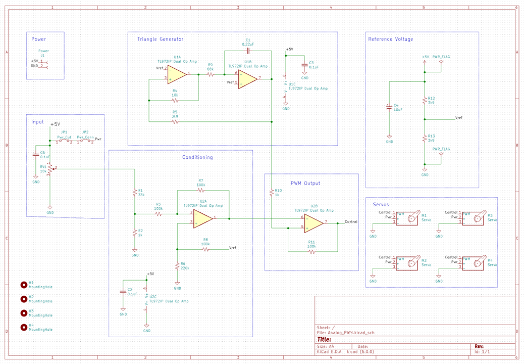
Schematic

Time for me to get my act together.  I put together a plan with the following approach:

  • Break the circuit into logical sections that can be tested sequentially
  • Describe the test plan for each section with the expected outcome
  • Solder it up a section at a time and test the section before moving on

The actual plan used is shown below.
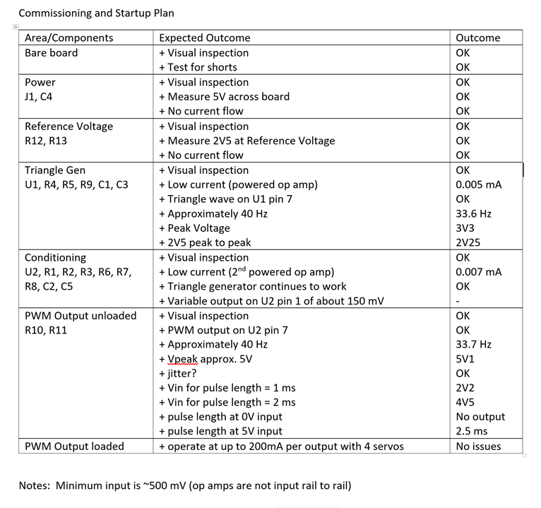
Commissioning and Startup Plan

One lesson from this was that the test plan should have been made before the PCB was sent out which would have allowed for dedicated test points.  Not shown in the plan (but they should have been) are the bench power over-voltage and over-current settings.

Fortunately, this board went together and started up without a problem but it got me thinking.  What did I leave out?  What tips do you have for planning and starting up an untested circuit?  Do you know of any good resources on the web?

  • Sign in to reply
  • Cancel

Top Replies

  • michaelkellett
    michaelkellett over 3 years ago +5
    For production designs of products which will be small and use 0402 parts I often start with a development or prototype board based on 0603 minimum sizes. I use lots of test points for power and key…
  • wolfgangfriedrich
    wolfgangfriedrich over 3 years ago +4
    With the small footprints on ICs, one can often measure correct solder joints on digital IOs or generally all pins that have protection diodes built in. With the DMM set to diode forward voltage mode,…
  • fmilburn
    fmilburn over 3 years ago in reply to BigG +3
    I had the same questions on test points, although it isn't clearly stated. How many, where to put them, and what to measure is the main reason I developed the test plan. I did some internet searching before…
Parents
  • BigG
    BigG over 3 years ago

    Hmm interesting.

    fmilburn said:
    What did I leave out? 

    I suppose this is side question... as in what's best practice for including test points on a PCB... I see shabaz has already touched on this in one of his comments.

    In particular I am curious to understand the following... What size should a test point be? How many to include? Where to place them? What to avoid? What do you measure etc.

    • Cancel
    • Vote Up +1 Vote Down
    • Sign in to reply
    • Cancel
Reply
  • BigG
    BigG over 3 years ago

    Hmm interesting.

    fmilburn said:
    What did I leave out? 

    I suppose this is side question... as in what's best practice for including test points on a PCB... I see shabaz has already touched on this in one of his comments.

    In particular I am curious to understand the following... What size should a test point be? How many to include? Where to place them? What to avoid? What do you measure etc.

    • Cancel
    • Vote Up +1 Vote Down
    • Sign in to reply
    • Cancel
Children
  • dougw
    dougw over 3 years ago in reply to BigG

    A lot depends on how much space you have. A test point could be a small surface pad or a though hole big enough to fit a DVM probe or it could be an actual component like a wire loop or connector jack. They should be on all power rails, and all signals of interest.

    • Cancel
    • Vote Up +2 Vote Down
    • Sign in to reply
    • Cancel
  • fmilburn
    fmilburn over 3 years ago in reply to BigG

    I had the same questions on test points, although it isn't clearly stated.  How many, where to put them, and what to measure is the main reason I developed the test plan.  I did some internet searching before making this post and what I found wasn't that enlightening.

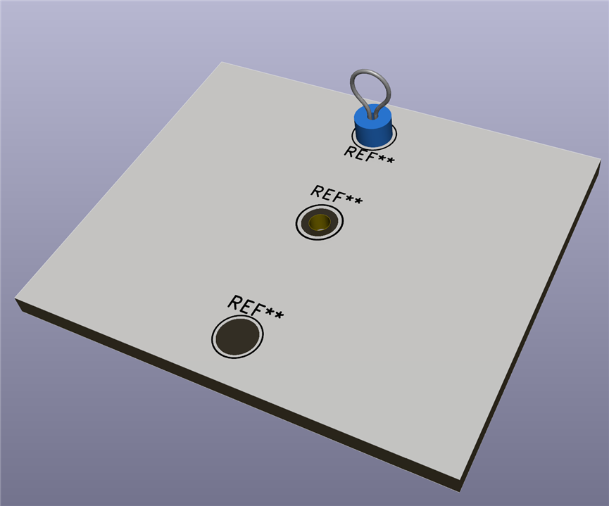
    KiCad has a number of footprints in the library.  A couple of them are shown below.

    Test Point Footprints

    I have tested a few PCBs in the RoadTest program with the loops and really like them for their ease of use.  Farnell / Newark carry them.  For example, there is Buy Now in different colors.

    • Cancel
    • Vote Up +3 Vote Down
    • Sign in to reply
    • Cancel
  • fmilburn
    fmilburn over 3 years ago in reply to dougw

    "They should be on all power rails, and all signals of interest"

    Well stated :-)  The signals of interest is the part I struggle with.  Making a test plan made me think about it and narrow the locations down - experience would be of great help here. One nice thing about through-hole parts is that it is pretty easy to probe almost anything.  SMD not always so much.  

    • Cancel
    • Vote Up +1 Vote Down
    • Sign in to reply
    • Cancel
  • Andrew J
    Andrew J over 3 years ago in reply to fmilburn

    Those are the ones I'm talking about as well.  The link you provide errors for me: incorrect link or not available in your country.  It may be worth posting the full URL.

    I always position them in pairs with one connected to ground and the other to the signal of interest.  The spacing I set as sufficient to allow me to use a probe and pigtail inserted into the loops, useful for minimising loops if checking for, e.g. ripple.  The through holes are sized to take those test points but are also just big enough to take the probe tip of my Siglent probes.  I've also found they are big enough to take a bootlace ferrule which is stopped by the ferrule 'flare' and makes a good connection without soldering.  The advantage is that the probe and pigtail insert into the ferrule and are held in place, even when placed vertically.  Ferrules are also dirt cheap.

    • Cancel
    • Vote Up +3 Vote Down
    • Sign in to reply
    • Cancel
  • fmilburn
    fmilburn over 3 years ago in reply to fmilburn

    I had the same questions on test points, although it isn't clearly stated.  How many, where to put them, and what to measure is the main reason I developed the test plan.  I did some internet searching before making this post and what I found wasn't that enlightening.

    KiCad has a number of footprints in the library.  A couple of them are shown below.

    Test Point Footprints

    I have tested a few PCBs in the RoadTest program with the loops and really like them for their ease of use.  Farnell / Newark carry them.  For example, there is Buy Now  in different colors.

    Here is another link if the one above doesn't work for you: TEST-1(BK) - Multicomp - PCB Test Point, Pin, Black (newark.com)

    • Cancel
    • Vote Up +1 Vote Down
    • Sign in to reply
    • Cancel
  • BigG
    BigG over 3 years ago in reply to fmilburn

    Thanks. Those loops will be very handy... which leads on to another question. What probes work best...

    • Cancel
    • Vote Up 0 Vote Down
    • Sign in to reply
    • Cancel
  • colporteur
    colporteur over 3 years ago in reply to BigG

    I use the 2.54 header pins for test points. You can use the straight or the right angle depending on the need. I set the hole for the pin in the PCB layout and the silkscreen but don't necessarily place the pin in production. On the first production run, you have all the pins but as you become familiar with the board, some points don't prove out as you hoped. Having the hole to place the pin that you don't use doesn't cost you anything.

    • Cancel
    • Vote Up 0 Vote Down
    • Sign in to reply
    • Cancel
  • Andrew J
    Andrew J over 3 years ago in reply to BigG

    Any really.  I use micro-grabbers with my DMM and normal scope probes.  As I mention, if you position two close together you can even use your scope probe with the pigtail attached.

    • Cancel
    • Vote Up +1 Vote Down
    • Sign in to reply
    • Cancel
  • dougw
    dougw over 3 years ago in reply to BigG

    I usually design the test points to accommodate the probes I have, usually a DVM or an oscilloscope.

    • Cancel
    • Vote Up 0 Vote Down
    • Sign in to reply
    • Cancel
element14 Community

element14 is the first online community specifically for engineers. Connect with your peers and get expert answers to your questions.

  • Members
  • Learn
  • Technologies
  • Challenges & Projects
  • Products
  • Store
  • About Us
  • Feedback & Support
  • FAQs
  • Terms of Use
  • Privacy Policy
  • Legal and Copyright Notices
  • Sitemap
  • Cookies

An Avnet Company © 2025 Premier Farnell Limited. All Rights Reserved.

Premier Farnell Ltd, registered in England and Wales (no 00876412), registered office: Farnell House, Forge Lane, Leeds LS12 2NE.

ICP 备案号 10220084.

Follow element14

  • X
  • Facebook
  • linkedin
  • YouTube