element14 Community
element14 Community
    Register Log In
  • Site
  • Search
  • Log In Register
  • About Us
  • Community Hub
    Community Hub
    • What's New on element14
    • Feedback and Support
    • Benefits of Membership
    • Personal Blogs
    • Members Area
    • Achievement Levels
  • Learn
    Learn
    • Ask an Expert
    • eBooks
    • element14 presents
    • Learning Center
    • Tech Spotlight
    • STEM Academy
    • Webinars, Training and Events
    • Learning Groups
  • Technologies
    Technologies
    • 3D Printing
    • FPGA
    • Industrial Automation
    • Internet of Things
    • Power & Energy
    • Sensors
    • Technology Groups
  • Challenges & Projects
    Challenges & Projects
    • Design Challenges
    • element14 presents Projects
    • Project14
    • Arduino Projects
    • Raspberry Pi Projects
    • Project Groups
  • Products
    Products
    • Arduino
    • Avnet Boards Community
    • Dev Tools
    • Manufacturers
    • Multicomp Pro
    • Product Groups
    • Raspberry Pi
    • RoadTests & Reviews
  • Store
    Store
    • Visit Your Store
    • Choose another store...
      • Europe
      •  Austria (German)
      •  Belgium (Dutch, French)
      •  Bulgaria (Bulgarian)
      •  Czech Republic (Czech)
      •  Denmark (Danish)
      •  Estonia (Estonian)
      •  Finland (Finnish)
      •  France (French)
      •  Germany (German)
      •  Hungary (Hungarian)
      •  Ireland
      •  Israel
      •  Italy (Italian)
      •  Latvia (Latvian)
      •  
      •  Lithuania (Lithuanian)
      •  Netherlands (Dutch)
      •  Norway (Norwegian)
      •  Poland (Polish)
      •  Portugal (Portuguese)
      •  Romania (Romanian)
      •  Russia (Russian)
      •  Slovakia (Slovak)
      •  Slovenia (Slovenian)
      •  Spain (Spanish)
      •  Sweden (Swedish)
      •  Switzerland(German, French)
      •  Turkey (Turkish)
      •  United Kingdom
      • Asia Pacific
      •  Australia
      •  China
      •  Hong Kong
      •  India
      •  Korea (Korean)
      •  Malaysia
      •  New Zealand
      •  Philippines
      •  Singapore
      •  Taiwan
      •  Thailand (Thai)
      • Americas
      •  Brazil (Portuguese)
      •  Canada
      •  Mexico (Spanish)
      •  United States
      Can't find the country/region you're looking for? Visit our export site or find a local distributor.
  • Translate
  • Profile
  • Settings
Experts, Learning and Guidance
  • Technologies
  • More
Experts, Learning and Guidance
Ask an Expert Forum How do you start up an untested circuit board?
  • Blog
  • Forum
  • Documents
  • Leaderboard
  • Files
  • Members
  • Mentions
  • Sub-Groups
  • Tags
  • More
  • Cancel
  • New
Join Experts, Learning and Guidance to participate - click to join for free!
Actions
  • Share
  • More
  • Cancel
Forum Thread Details
  • Replies 38 replies
  • Subscribers 287 subscribers
  • Views 7321 views
  • Users 0 members are here
  • testing
  • start-up
  • circuit board
Related
See a helpful answer?

Be sure to click 'more' and select 'suggest as answer'!

If you're the thread creator, be sure to click 'more' then 'Verify as Answer'!

How do you start up an untested circuit board?

fmilburn
fmilburn over 3 years ago

I've been known to throw a circuit together, apply power to it, and fry something.  Or the circuit just doesn't work and the problem could be anywhere in that mess of wiring.  But I used to work on complex and potentially hazardous projects where we couldn't afford those types of mistakes. There were mechanical, electrical, civil, chemical processing, and instrumentation disciplines, and towards the middle of the design specialists in commissioning and start-up were brought in.

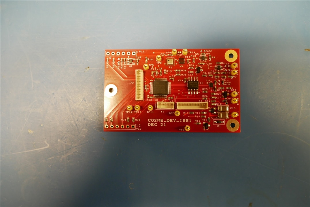
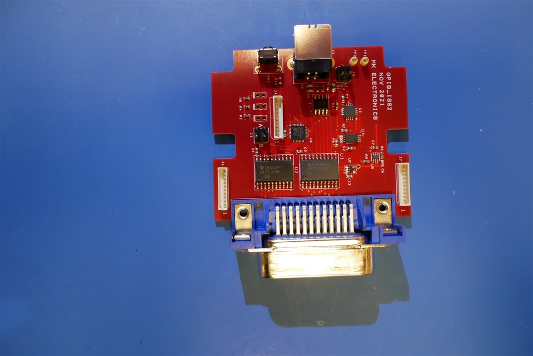
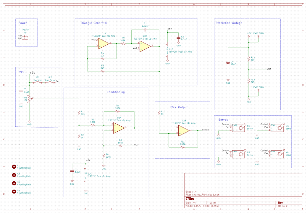
I recently sent out a PCB design for manufacture without prototyping it first.  The schematic is shown below but it is just an example.  My question is more general to starting up any untested circuits.

Schematic

Time for me to get my act together.  I put together a plan with the following approach:

  • Break the circuit into logical sections that can be tested sequentially
  • Describe the test plan for each section with the expected outcome
  • Solder it up a section at a time and test the section before moving on

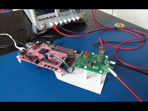
The actual plan used is shown below.

Commissioning and Startup Plan

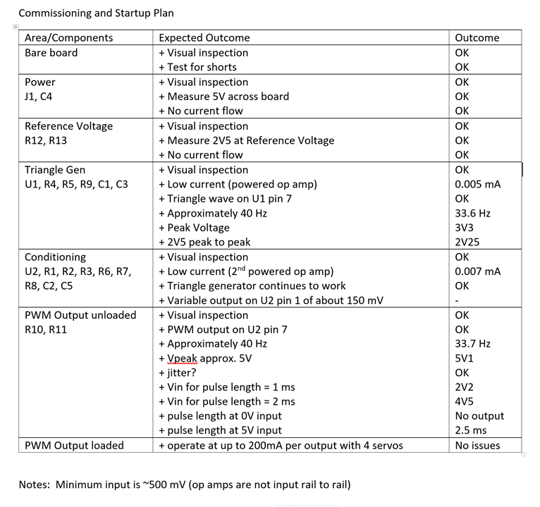
One lesson from this was that the test plan should have been made before the PCB was sent out which would have allowed for dedicated test points.  Not shown in the plan (but they should have been) are the bench power over-voltage and over-current settings.

Fortunately, this board went together and started up without a problem but it got me thinking.  What did I leave out?  What tips do you have for planning and starting up an untested circuit?  Do you know of any good resources on the web?

  • Sign in to reply
  • Cancel

Top Replies

  • michaelkellett
    michaelkellett over 3 years ago +5
    For production designs of products which will be small and use 0402 parts I often start with a development or prototype board based on 0603 minimum sizes. I use lots of test points for power and key…
  • wolfgangfriedrich
    wolfgangfriedrich over 3 years ago +4
    With the small footprints on ICs, one can often measure correct solder joints on digital IOs or generally all pins that have protection diodes built in. With the DMM set to diode forward voltage mode,…
  • fmilburn
    fmilburn over 3 years ago in reply to BigG +3
    I had the same questions on test points, although it isn't clearly stated. How many, where to put them, and what to measure is the main reason I developed the test plan. I did some internet searching before…
Parents
  • michaelkellett
    michaelkellett over 3 years ago

    For production designs of products which will be small and use 0402 parts I often start with a development or prototype board based on 0603 minimum sizes.

    I use lots of test points for power and key analogue signals. I use little Molex picoblade 10 way connectors for digital stuff (pins 1 and 10 are ground and 8 signals in between). I can connect these with simple adapter leads to a logic analyser.

    SPI and I2C buses often cause problems so I like to take them out on a connector and generally try and make sure that any spare pins on an FPGA or processor are connected to a debug connector.

    On things that will only be built in smallish numbers (<100) then I would leave all the debug stuff on the final design.

    This is a prototype board, the real device will fit in the space defined by PL1 and 2. None of the Molex connectors or test pins will be retained.

    image

    This is a GPIB or IEE-488 to USB interface board. I won't ever make that many so the test pins and debug connectors will stay forever.

    image

    MK

    • Cancel
    • Vote Up +5 Vote Down
    • Sign in to reply
    • Cancel
  • fmilburn
    fmilburn over 3 years ago in reply to michaelkellett

    Thanks Michael,

    I have come to the realization that I should be providing more test points. 

    • Cancel
    • Vote Up +1 Vote Down
    • Sign in to reply
    • Cancel
  • wolfgangfriedrich
    wolfgangfriedrich over 3 years ago in reply to fmilburn

    This statement is universally true. 

    And something else I just remembered (which has to happen during layout), if there is space on the board, more text is also always appreciated by oneself when bringing the board up. With the designator also a net name to every testpoint. Signals to connector pin. Also very important a visible pin 1 marker at all connectors, ICs, more-than-3-pin-components. Function of jumpers in text. Also useful for high pin count ICs, every 5th pin a little dot and every 10th pin a little line (flashback when QFP-144 was a lot of pins).  Also more GND pins with label, to clip GND probes to the board close to the measuring pins. 

    Unrelated, if the board has mounting holes, small nylon stand-offs are useful to raise the board above the work surface to prevent anything on the bottom side make contact with little conductive pieces lying on my messy workbench. 

    • Cancel
    • Vote Up +3 Vote Down
    • Sign in to reply
    • Cancel
Reply
  • wolfgangfriedrich
    wolfgangfriedrich over 3 years ago in reply to fmilburn

    This statement is universally true. 

    And something else I just remembered (which has to happen during layout), if there is space on the board, more text is also always appreciated by oneself when bringing the board up. With the designator also a net name to every testpoint. Signals to connector pin. Also very important a visible pin 1 marker at all connectors, ICs, more-than-3-pin-components. Function of jumpers in text. Also useful for high pin count ICs, every 5th pin a little dot and every 10th pin a little line (flashback when QFP-144 was a lot of pins).  Also more GND pins with label, to clip GND probes to the board close to the measuring pins. 

    Unrelated, if the board has mounting holes, small nylon stand-offs are useful to raise the board above the work surface to prevent anything on the bottom side make contact with little conductive pieces lying on my messy workbench. 

    • Cancel
    • Vote Up +3 Vote Down
    • Sign in to reply
    • Cancel
Children
  • Jan Cumps
    Jan Cumps over 3 years ago in reply to wolfgangfriedrich
    wolfgangfriedrich said:
    if the board has mounting holes, small nylon stand-offs are useful

    Yes. I bought some assorted nylon bolts and nuts that I use and reuse. 

    Sometimes to lift the board. Sometimes I put two boards, that I need to interconnect with jumpers,  on a piece of cardboard, so that they don't move. Or a combination, like here:

    image

    • Cancel
    • Vote Up +2 Vote Down
    • Sign in to reply
    • Cancel
  • colporteur
    colporteur over 3 years ago in reply to Jan Cumps

    That one impressively clean bench! Where are the bits of wire insulation and scattered food crumbs?

    • Cancel
    • Vote Up +1 Vote Down
    • Sign in to reply
    • Cancel
element14 Community

element14 is the first online community specifically for engineers. Connect with your peers and get expert answers to your questions.

  • Members
  • Learn
  • Technologies
  • Challenges & Projects
  • Products
  • Store
  • About Us
  • Feedback & Support
  • FAQs
  • Terms of Use
  • Privacy Policy
  • Legal and Copyright Notices
  • Sitemap
  • Cookies

An Avnet Company © 2025 Premier Farnell Limited. All Rights Reserved.

Premier Farnell Ltd, registered in England and Wales (no 00876412), registered office: Farnell House, Forge Lane, Leeds LS12 2NE.

ICP 备案号 10220084.

Follow element14

  • X
  • Facebook
  • linkedin
  • YouTube