element14 Community
element14 Community
    Register Log In
  • Site
  • Search
  • Log In Register
  • Community Hub
    Community Hub
    • What's New on element14
    • Feedback and Support
    • Benefits of Membership
    • Personal Blogs
    • Members Area
    • Achievement Levels
  • Learn
    Learn
    • Ask an Expert
    • eBooks
    • element14 presents
    • Learning Center
    • Tech Spotlight
    • STEM Academy
    • Webinars, Training and Events
    • Learning Groups
  • Technologies
    Technologies
    • 3D Printing
    • FPGA
    • Industrial Automation
    • Internet of Things
    • Power & Energy
    • Sensors
    • Technology Groups
  • Challenges & Projects
    Challenges & Projects
    • Design Challenges
    • element14 presents Projects
    • Project14
    • Arduino Projects
    • Raspberry Pi Projects
    • Project Groups
  • Products
    Products
    • Arduino
    • Avnet & Tria Boards Community
    • Dev Tools
    • Manufacturers
    • Multicomp Pro
    • Product Groups
    • Raspberry Pi
    • RoadTests & Reviews
  • About Us
    About the element14 Community
  • Store
    Store
    • Visit Your Store
    • Choose another store...
      • Europe
      •  Austria (German)
      •  Belgium (Dutch, French)
      •  Bulgaria (Bulgarian)
      •  Czech Republic (Czech)
      •  Denmark (Danish)
      •  Estonia (Estonian)
      •  Finland (Finnish)
      •  France (French)
      •  Germany (German)
      •  Hungary (Hungarian)
      •  Ireland
      •  Israel
      •  Italy (Italian)
      •  Latvia (Latvian)
      •  
      •  Lithuania (Lithuanian)
      •  Netherlands (Dutch)
      •  Norway (Norwegian)
      •  Poland (Polish)
      •  Portugal (Portuguese)
      •  Romania (Romanian)
      •  Russia (Russian)
      •  Slovakia (Slovak)
      •  Slovenia (Slovenian)
      •  Spain (Spanish)
      •  Sweden (Swedish)
      •  Switzerland(German, French)
      •  Turkey (Turkish)
      •  United Kingdom
      • Asia Pacific
      •  Australia
      •  China
      •  Hong Kong
      •  India
      •  Japan
      •  Korea (Korean)
      •  Malaysia
      •  New Zealand
      •  Philippines
      •  Singapore
      •  Taiwan
      •  Thailand (Thai)
      •  Vietnam
      • Americas
      •  Brazil (Portuguese)
      •  Canada
      •  Mexico (Spanish)
      •  United States
      Can't find the country/region you're looking for? Visit our export site or find a local distributor.
  • Translate
  • Profile
  • Settings
Open Source Hardware
  • Technologies
  • More
Open Source Hardware
Blog Discrete difference amplifier - AC analysis: gain and bandwidth
  • Blog
  • Forum
  • Documents
  • Events
  • Polls
  • Members
  • Mentions
  • Sub-Groups
  • Tags
  • More
  • Cancel
  • New
Join Open Source Hardware to participate - click to join for free!
  • Share
  • More
  • Cancel
Group Actions
  • Group RSS
  • More
  • Cancel
Engagement
  • Author Author: Jan Cumps
  • Date Created: 14 Jul 2026 6:26 PM Date Created
  • Views 312 views
  • Likes 7 likes
  • Comments 13 comments
  • simple_dcr
Related
Recommended

Discrete difference amplifier - AC analysis: gain and bandwidth

Jan Cumps
Jan Cumps
14 Jul 2026

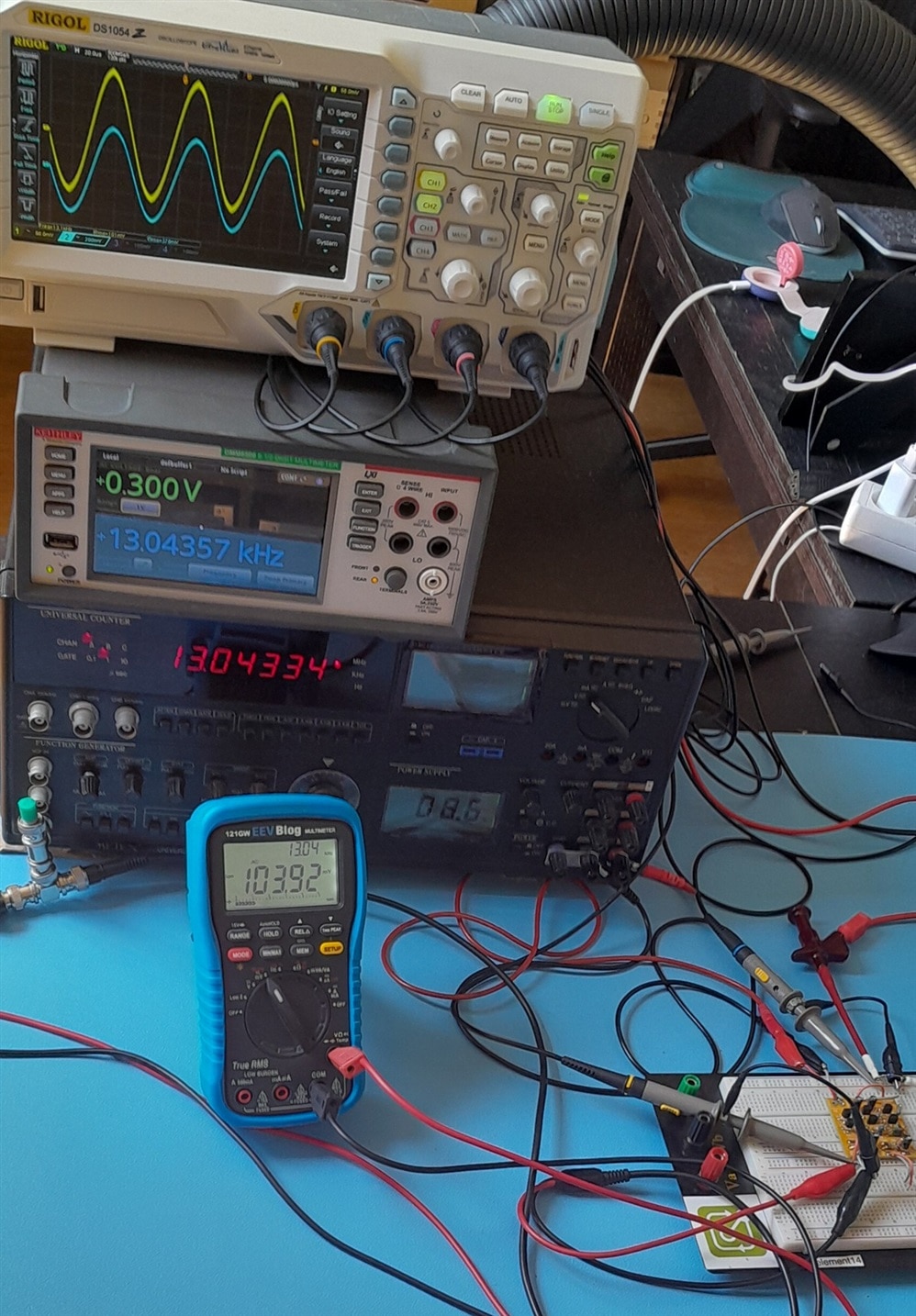
This is the AC gain and BW analysis of the difference amplifier module that shabaz designed for a Direct Conversion Receiver.

image

I'm searching for these points:

  • gain at 1 kHz (approx. mid of bandwidth)
  • -3 dB frequencies

I use Vrms values in the post - common for audio circuits. When measuring one of the differential channels, I tie the other to ground.
image

Specs:

  • Gain: ~10 dB
  • Bandwidth (-3 dB): ~30 Hz to 40 kHz (approximate)

Measurements:
image

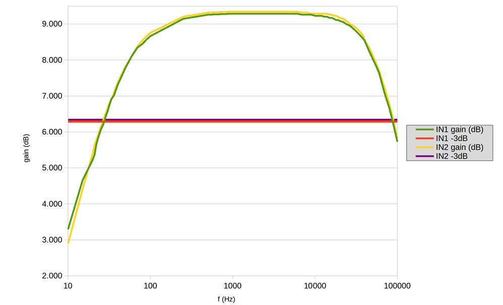
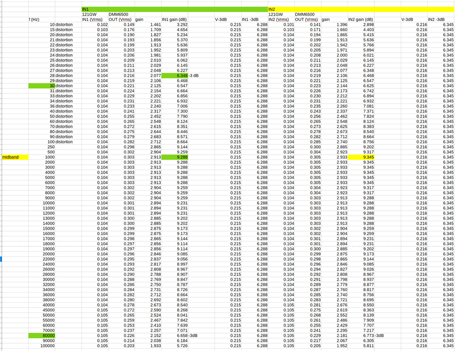
IN1: gain (1 kHz): 9.2 dB, bw (-3 dB): 30 Hz - 80 kHz

IN2: gain (1 kHz): 9.3 dB, bw (-3 dB): 30 Hz - 80 kHz
image

 shabaz published the KiCad project on GitHub, including simulation. You could load it into KiCad and check if the small signal simulation and my measurements match ...

For all blog posts in this series, click here

spreadsheet: differenceamp.zip

  • Sign in to reply
Parents
  • Jan Cumps
    Jan Cumps 1 month ago

    For the next blog, I plan to

    • show some internal signals
    • test how the circuit behaves when there is an identical signal on both inputs (desired/theoretical result: no output signal)
    • go into the design, maybe based on Art of Electronics:

    image

    • Cancel
    • Vote Up 0 Vote Down
    • Sign in to reply
    • More
    • Cancel
  • jc2048
    jc2048 14 days ago in reply to Jan Cumps

    Does AoE say how you use the 'active load', or do they just give you that partial schematic?

    It's not going to work well open loop - the operating point and the gain that results as the two sources (the mirror output and the diff pair output) fight comes from the slopes specified by the Early voltages, and they're not well characterised, and not necessarily balanced between the PNP and the NPN part. [It works best used with further stages and then overall feedback to determine the operating point and the actual, precise gain.]

    Besides which, that's not how Shabaz is using the mirror, anyhow. He's got it the other way round so that it's mirroring the output current that flows in the passive resistor load as feedback to the other transistor in the diff pair. It's unconventional, and I'm not very sure what all the consequences of doing that might be. It seems to give a small amount of loop gain (which we might expect to [slightly] improve the distortion performance (maybe not - the diode-connected transistor at the mirror input is itself a major source of distortion in the output), lower the output impedance, maybe give some PSRR, and all those kinds of benefits that you get from feedback). The biggest obvious problem is the higher gain on the left side will drive the other diff pair transistor into the saturation region with larger input signals, compromise the operation of the diff pair, and result in the sudden onset of output distortion. And it's all a bit uncontrolled, and most definitely the simulation won't get it right because the Early voltages in the transistor models probably won't be very typical of the actual parts.

    If you view an FFT of the output, do you see the output distortion suddenly rise at some point as you increase the signal level? It should be around the same point that the waveform on the other side limits against the lower transistor collector.

    As to the current source in the tail of the diff pair, the two transistors would lead to a higher slope on the current vs voltage characteristic, which you would think would result in more output distortion (over the simpler, one-transistor sink), but maybe Shabaz was adjusting that to partially counter one of the other distortion sources.

    • Cancel
    • Vote Up 0 Vote Down
    • Sign in to reply
    • More
    • Cancel
  • Jan Cumps
    Jan Cumps 11 days ago in reply to jc2048

    Does AoE say how you use the 'active load', or do they just give you that partial schematic?

    They elaborate on the current source and on the active load. The dedicated subsection "Biasing with a current source" and "Current-mirror active load" give (short) background.

    I'll do the extra measurements when the heat wave is over...

    • Cancel
    • Vote Up 0 Vote Down
    • Sign in to reply
    • More
    • Cancel
Comment
  • Jan Cumps
    Jan Cumps 11 days ago in reply to jc2048

    Does AoE say how you use the 'active load', or do they just give you that partial schematic?

    They elaborate on the current source and on the active load. The dedicated subsection "Biasing with a current source" and "Current-mirror active load" give (short) background.

    I'll do the extra measurements when the heat wave is over...

    • Cancel
    • Vote Up 0 Vote Down
    • Sign in to reply
    • More
    • Cancel
Children
No Data
element14 Community

element14 is the first online community specifically for engineers. Connect with your peers and get expert answers to your questions.

  • Members
  • Learn
  • Technologies
  • Challenges & Projects
  • Products
  • Store
  • About Us
  • Feedback & Support
  • FAQs
  • Terms of Use
  • Privacy Policy
  • Legal and Copyright Notices
  • Sitemap
  • Cookies

An Avnet Company © 2026 Premier Farnell Limited. All Rights Reserved.

Premier Farnell Ltd, registered in England and Wales (no 00876412), registered office: Farnell House, Forge Lane, Leeds LS12 2NE.

Follow element14

  • X
  • Facebook
  • linkedin
  • YouTube