element14 Community
element14 Community
    Register Log In
  • Site
  • Search
  • Log In Register
  • Community Hub
    Community Hub
    • What's New on element14
    • Feedback and Support
    • Benefits of Membership
    • Personal Blogs
    • Members Area
    • Achievement Levels
  • Learn
    Learn
    • Ask an Expert
    • eBooks
    • element14 presents
    • Learning Center
    • Tech Spotlight
    • STEM Academy
    • Webinars, Training and Events
    • Learning Groups
  • Technologies
    Technologies
    • 3D Printing
    • FPGA
    • Industrial Automation
    • Internet of Things
    • Power & Energy
    • Sensors
    • Technology Groups
  • Challenges & Projects
    Challenges & Projects
    • Design Challenges
    • element14 presents Projects
    • Project14
    • Arduino Projects
    • Raspberry Pi Projects
    • Project Groups
  • Products
    Products
    • Arduino
    • Avnet Boards Community
    • Dev Tools
    • Manufacturers
    • Multicomp Pro
    • Product Groups
    • Raspberry Pi
    • RoadTests & Reviews
  • About Us
  • Store
    Store
    • Visit Your Store
    • Choose another store...
      • Europe
      •  Austria (German)
      •  Belgium (Dutch, French)
      •  Bulgaria (Bulgarian)
      •  Czech Republic (Czech)
      •  Denmark (Danish)
      •  Estonia (Estonian)
      •  Finland (Finnish)
      •  France (French)
      •  Germany (German)
      •  Hungary (Hungarian)
      •  Ireland
      •  Israel
      •  Italy (Italian)
      •  Latvia (Latvian)
      •  
      •  Lithuania (Lithuanian)
      •  Netherlands (Dutch)
      •  Norway (Norwegian)
      •  Poland (Polish)
      •  Portugal (Portuguese)
      •  Romania (Romanian)
      •  Russia (Russian)
      •  Slovakia (Slovak)
      •  Slovenia (Slovenian)
      •  Spain (Spanish)
      •  Sweden (Swedish)
      •  Switzerland(German, French)
      •  Turkey (Turkish)
      •  United Kingdom
      • Asia Pacific
      •  Australia
      •  China
      •  Hong Kong
      •  India
      •  Korea (Korean)
      •  Malaysia
      •  New Zealand
      •  Philippines
      •  Singapore
      •  Taiwan
      •  Thailand (Thai)
      • Americas
      •  Brazil (Portuguese)
      •  Canada
      •  Mexico (Spanish)
      •  United States
      Can't find the country/region you're looking for? Visit our export site or find a local distributor.
  • Translate
  • Profile
  • Settings
Open Source Hardware
  • Technologies
  • More
Open Source Hardware
Blog High Voltage Isolated Measurement Board: Initial Prototype
  • Blog
  • Forum
  • Documents
  • Events
  • Polls
  • Members
  • Mentions
  • Sub-Groups
  • Tags
  • More
  • Cancel
  • New
Join Open Source Hardware to participate - click to join for free!
  • Share
  • More
  • Cancel
Group Actions
  • Group RSS
  • More
  • Cancel
Engagement
  • Author Author: shabaz
  • Date Created: 13 Dec 2023 9:10 PM Date Created
  • Views 3211 views
  • Likes 9 likes
  • Comments 7 comments
  • high voltage
  • voltage measurement
  • isolation
  • optoisolator
Related
Recommended

High Voltage Isolated Measurement Board: Initial Prototype

shabaz
shabaz
13 Dec 2023
High Voltage Isolated Measurement Board: Initial Prototype

Introduction

In an earlier blog post  Very Low-Cost Pulse-Width Modulation (PWM), and Isolated Analog Measurements  a method was discussed to perform isolated analog measurements at a sub-£1/$1 price. It was fine for slow-changing signals, but I wanted something that could be used at up to say 100 kHz too.

This blog post discusses the work done so far. Note: it is not a functioning project, it is still a work-in-progress, with some known faults, and probably some unknown ones too. Please do not apply it to high voltages yet, it could damage test equipment or cause other harm. It has barely been tested, but the information is here in case anyone wishes to help debug!

The aim of this project is to have a circuit that can be used to monitor up to a kV or so, with high input impedance, and, as mentioned, at up to around 100 kHz bandwidth. This could be useful for testing out high voltage control loops or for general measurement of high voltages.

Circuit

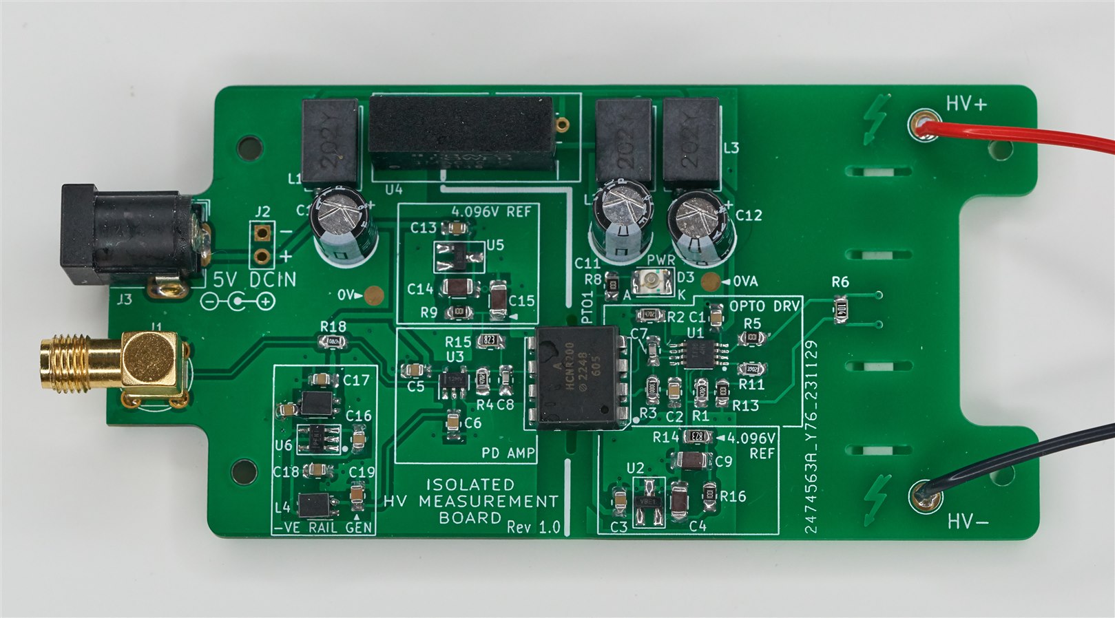
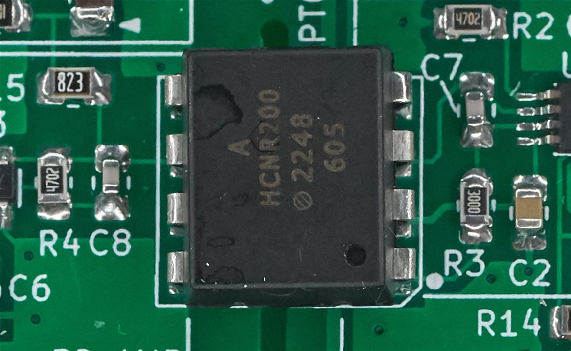
The proposed circuit revolves around a special linear optocoupler (see the HCNR200 PDF datasheet), which contains one LED and two identical photodiodes, which are used for feedback into op-amps on both sides of the isolation barrier.

On the input side, a potential divider is used to reduce the high voltage down to something that can be buffered by op-amp U1A, and then U1B is used to control the LED inside the optocoupler, using one of the photodiodes as feedback for it. OPA2197 and OPA197 op amps (PDF datasheet) are used in this project.

On the output side, the other photodiode is used, to provide a linear output voltage using an isolated op-amp. Most of the design decisions are already discussed, in the comments in the earlier blog. The circuit as shown is intended for input voltages in the range of -550V to +550V, but the range can be altered with component changes.

image


Building It

To build the board, check out the GitHub repository, which contains the PCB Gerber files, and a PDF parts list and PDF schematic . You could download the entire repo and get access to the KiCad files too. The board assembly was easy by simply printing out the parts list and following that.
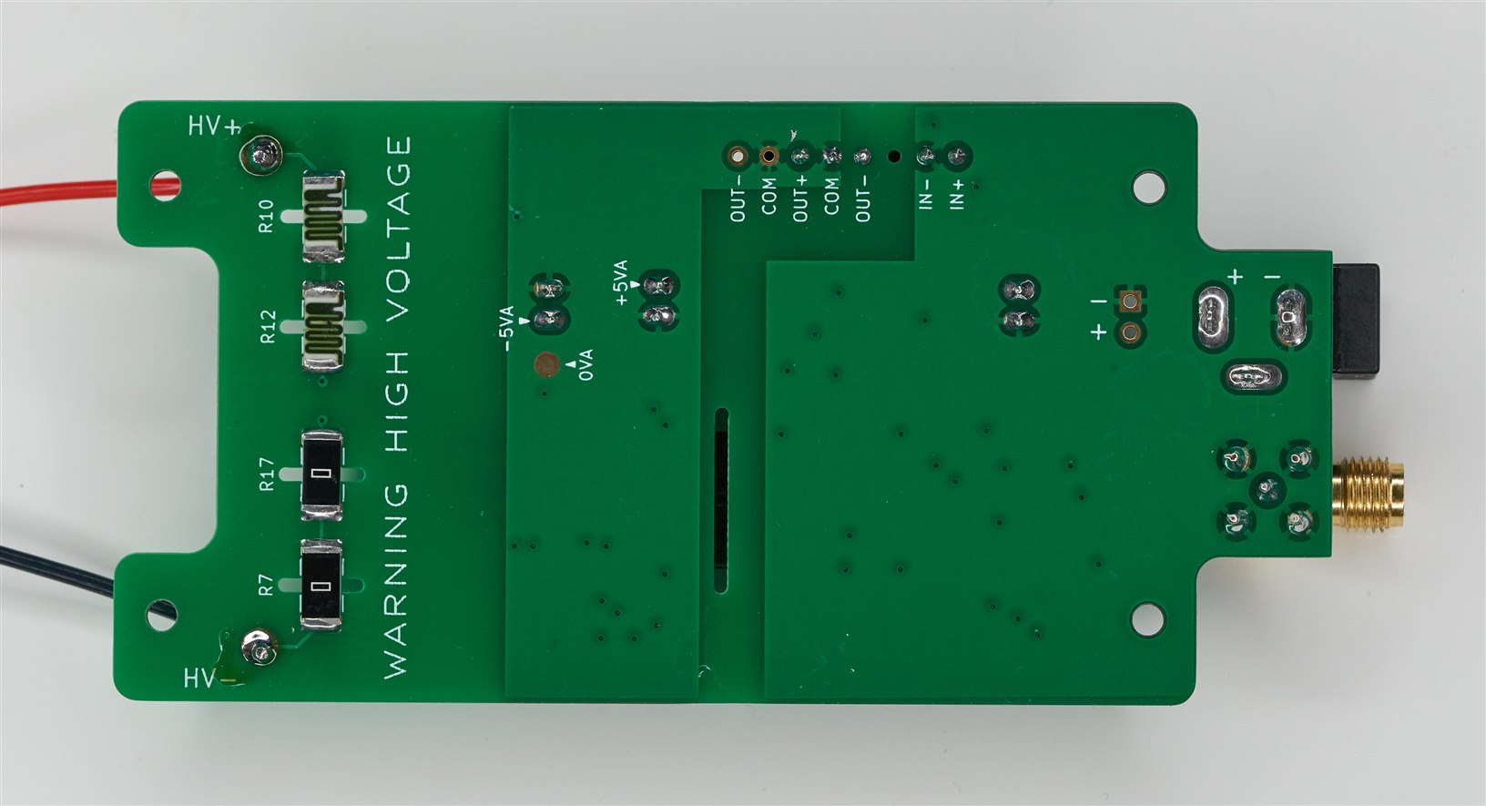
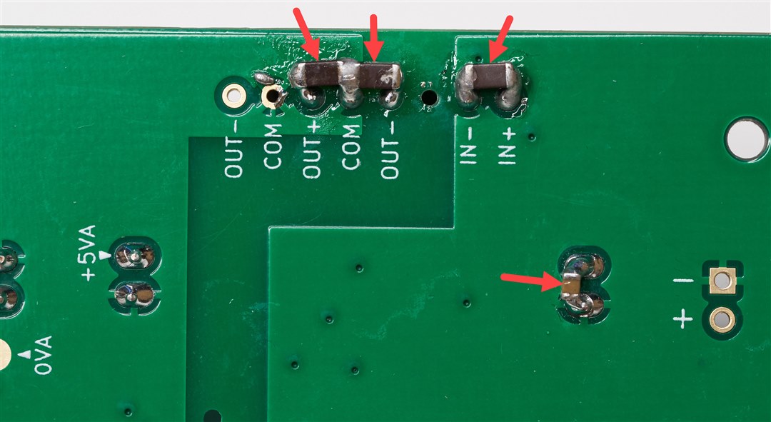
image

Board underside:

image


Issues

1. One immediate problem that will be encountered when assembling the board, is that the most important part (the optocoupler!) is wider than the footprint on the PCB : ( I don’t know how I messed that up. The fix is easy on the Rev 1 board; fold in the legs of the optocoupler using pliers, pushing the legs inwards.

image

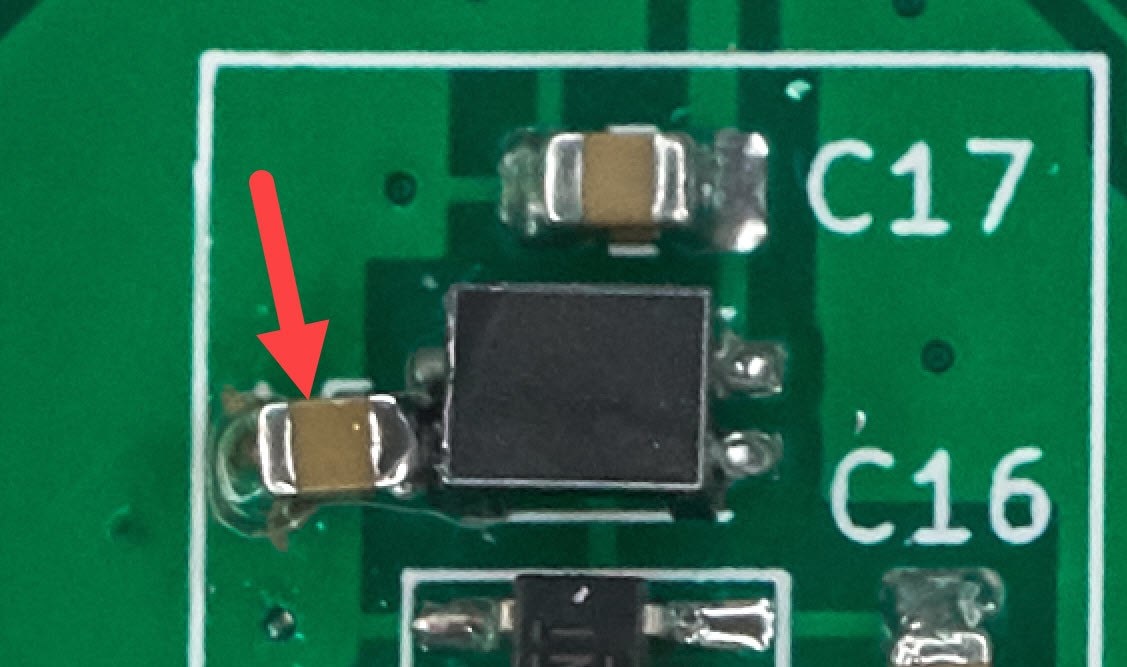
2. When powered up, the current was high! And the negative rail was not very negative. It was a silly mistake; the negative rail generator IC (TPS60403 PDF datasheet) needs an input decoupling capacitor; the impedance from the input choke will cause issues with such switched capacitor circuits. The fix was to solder on a 1uF capacitor, one end soldered to the choke, and the other soldered to 0V. I had to scratch off the solder mask on the 0V copper pour to perform this fix.

image

3. This issue I still need to get to the bottom of. There is a signal (about 72 kHz) on the output, at about 40 mV p-p. The DC-DC converter (TMA 0505D) is operating in this frequency region, the output voltage from the DC-DC converter is about +5.2V and -5.2V so I don’t think anything is dropping out, but I think it is being coupled at the input. I have not debugged this sufficiently yet.

image

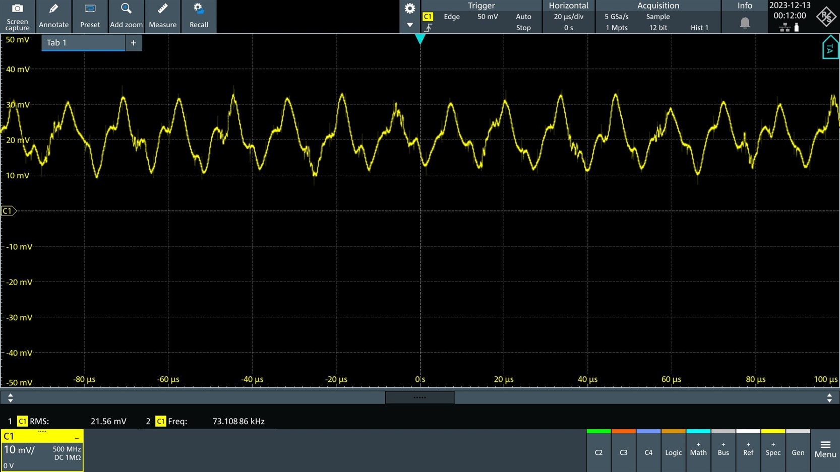
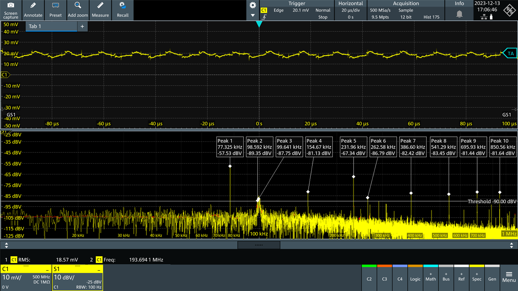
Reducing the potential divider resistor R6 from 100k down to 10k certainly reduces the signal (see the screenshot below), so I think it is coupling of some sort. It may even need a new PCB layout and further distance from the DC-DC converter : ( (this is just speculation, as mentioned, I have not got far in debugging this yet at all).

image

However I have added additional decoupling capacitors around the DC-DC converter (by soldering ceramic capacitors on the underside of the board), but that didn’t make a noticeable difference.

image

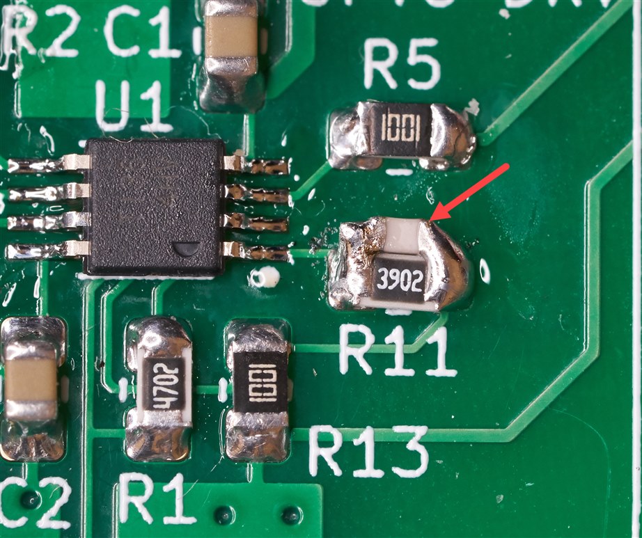
Also, it would probably be a good idea to reduce input buffer/amp bandwidth a little bit by soldering a capacitor (a few pF) across R11 in a future board layout, but for now, I tried it and there’s no noticeable difference for now, since the larger signal is so visible.

image

Also, it would be very good to have some sort of transient protection across the input supply rail, in case of any capacitively coupled signal from the high voltage side via the DC-DC converter.

Next Steps

I did briefly apply a voltage at the input and observed the correct output, so at least that part is functioning. However as can be seen from the scope outputs, work is clearly needed to resolve the unexpected signal issue. Also, at some point, it would be good to introduce offset nulling capability. I see a 20mV offset.

Any help would be appreciated. If you have ideas, let me know, and I can test it remotely. Or, if you wish to get your hands dirty and have some fun (hopefully) building it up (either entirely or bits of it) and troubleshooting, I have a few spare PCBs, and I’m happy to post them anywhere.

Once the board is functioning a bit better, I'll update the schematic and PCB, so that hopefully a revision 2 board can work much better. Eventually, the board could be fitted into the following enclosure if desired:

image 

(image source: Farnell website)

Thanks for reading!

  • Sign in to reply

Top Comments

  • jc2048
    jc2048 over 1 year ago +1
    Interesting project. For the noise signal, I'd take out the DC-DC converter and run it on something else (bench PSU or batteries). It will quickly show whether it's the source, regardless of how it might…
  • jc2048
    jc2048 over 1 year ago in reply to shabaz +1
    The opto LED doesn't really have much PSRR, does it? If anything, it might be a slight gain, as the curve is non-linear and a small change in the supply voltage will give a higher proportional change in…
  • jc2048
    jc2048 over 1 year ago in reply to shabaz +1
    There may be some variation in PSRR between op amps, but they all drop off as the frequency goes up (from a few hundred Hz up). I would think it's factors like the internal current sources not keeping…
  • jc2048
    jc2048 over 1 year ago in reply to shabaz

    There may be some variation in PSRR between op amps, but they all drop off as the frequency goes up (from a few hundred Hz up). I would think it's factors like the internal current sources not keeping up and internal capacitive coupling becoming a problem, and things like that, but I don't know for sure. At least the one you've chosen is balanced for +PSRR and -PSRR. A lot of older bipolar parts were quite unbalanced, with one rail much better than the other.

    This is what my simulation shows if I step the LED resistor 100R, 200R, 300R. No effect up to 100kHz, but the 300 is slightly better from there up.

    image

    • Cancel
    • Vote Up +1 Vote Down
    • Sign in to reply
    • More
    • Cancel
  • shabaz
    shabaz over 1 year ago in reply to jc2048

    Hi Jon,

    I believe it's related to supply noise for that LED and it's op-amp PSRR, but was also wondering if the op amp was able to control well at that combination of drive current and LED output and photodiode response, but varying that resistor makes no noticeable difference to the output. I could try a OPA2192 chip instead of OPA2197 for a slight improvement, but I don't know if that will help enough (the charts look identical in the datasheet , but in the electrical characteristics it shows there could be a 20dB improvement), since the charts look identical I will probably leave that for now.

    I am going to try a couple of 9V batteries (I have a low-noise +-5V regulator board to use with that), to see what happens.

    • Cancel
    • Vote Up 0 Vote Down
    • Sign in to reply
    • More
    • Cancel
  • jc2048
    jc2048 over 1 year ago in reply to shabaz

    The opto LED doesn't really have much PSRR, does it? If anything, it might be a slight gain, as the curve is non-linear and a small change in the supply voltage will give a higher proportional change in the current (which defines the light output). The one thing that might affect things is the intrinsic capacitance of the LED junction, but I don't think that will have a filtering effect until up into the MHz area.

    This is the PSRR simulated. This is purely indicative - there's no hope it accurately models what you've got because there's nothing there to model the effect of the supply distribution and decoupling.

    The green curve is LED and op amp running off noisy supply.
    The red curve is op amp noisy and LED perfectly clean.

    image
    I've only injected a signal into the +5V, so it's also only looking at part of what's going on. Looks like a factor of a little over 20, or so, between the two curves. The cursors are on 72kHz.

    So, it suggests there is at least some benefit to cleaning up the LED supply. [As a quick hack, as long as you keep the LED current to less than 8mA, you could try running the LED from the 4V reference output, just to see how much difference a cleaner supply makes, though 3x AA batteries would be even quieter.]

    The PSRR of the op amps is only mid 40s at that frequency, so local supply filtering close in to the op amp would probably be of benefit too. Even just a few ohms in front of the decoupling cap would probably help.

    Personally, I'd concentrate on a cleaner supply, though. Could the front end be made to work on a single PP3 if the fake earth was biased to give a bit more headroom on the positive side [perhaps +5V and -4V]?

    For anyone that's interested, this is the circuit in the simulator. The free TI Tina is sometimes a bit clunky with the parameter stepping and it doesn't seem to control switch settings, so instead I used a VCVS to mirror the 'noise' signal to the LED where I could use a gain of x0 or x1 to select either there or not there. Set to 'parameter stepping' mode, that then allowed me to have both curves on the same Bode plot.

    image

    • Cancel
    • Vote Up +1 Vote Down
    • Sign in to reply
    • More
    • Cancel
  • shabaz
    shabaz over 1 year ago in reply to jc2048

    Hi Jon,

    Great points! Compensation is definitely something that I'll need to consider.  I'm hoping the parasitic capacitance won't vary too much from board-to-board, to try to make it somewhat repeatable, but it may still need trimming due to capacitor tolerance. I H-field probed the DC-DC converter, and the field extends over a lot of the board, but I still wasn't sure if it was radiated or conducted issues, so I unsoldered the DC-DC converter and put it on extension wires, and that made absolutely no difference. Next I tried a fairly low-noise DIY supply (I couldn't use batteries for now because the 4.096V reference requires 5.5V max) and the output noise changed characteristics, so it is definitely influenced by the supplies. I connected the supply with as much ferrite as I could fit on the cable.

    The screenshot here shows the output noise on the SMA connector J1, with the DC-DC converter replaced by an external supply (this is with R6 being 10k, I need to replace it back to 100k).

    image

    I checked the noise of the external supply out-of-circuit (I measured this for now without a load, so it will be different in-circuit). This is the positive rail, about 277uV RMS noise according to the automated measurement at the bottom of the screen:

    image

    The negative rail is very similar:

    image

    I'm now speculating maybe the current through the LED needs to be altered, maybe there is a region where it could be less susceptible to power rail noise : ( But this will affect the dynamic range. Or, it needs a further order of magnitude lower-noise supply rails, perhaps by replacing the DC-DC converter to a +-9V output one, followed by more than one regulator! but this is getting to be excessive, it seems unusual that it should be so sensitive to the supply rail. The OPA2197 has reasonable PSRR too.

    • Cancel
    • Vote Up 0 Vote Down
    • Sign in to reply
    • More
    • Cancel
  • jc2048
    jc2048 over 1 year ago in reply to jc2048

    Ignore the part about the open-loop response. I had the circuit slightly wrong AND misremembered the result into the bargain.

    • Cancel
    • Vote Up 0 Vote Down
    • Sign in to reply
    • More
    • Cancel
>
element14 Community

element14 is the first online community specifically for engineers. Connect with your peers and get expert answers to your questions.

  • Members
  • Learn
  • Technologies
  • Challenges & Projects
  • Products
  • Store
  • About Us
  • Feedback & Support
  • FAQs
  • Terms of Use
  • Privacy Policy
  • Legal and Copyright Notices
  • Sitemap
  • Cookies

An Avnet Company © 2025 Premier Farnell Limited. All Rights Reserved.

Premier Farnell Ltd, registered in England and Wales (no 00876412), registered office: Farnell House, Forge Lane, Leeds LS12 2NE.

ICP 备案号 10220084.

Follow element14

  • X
  • Facebook
  • linkedin
  • YouTube