


To draw PCB layout is an essential ability for electronic engineer .
We could use many tools for PCB Layout , Altium Designer, Kicad, PADS,and so forth .But for a reason that these software are all desktop-based , you need to install it on your PC or may need to pay for the software .EasyEDA provides a feasible way to draw schematic and PCB online ,without installing a software on your PC , and you could also save it on the cloud server and share it to all the internet users in the meantime .You could utilize all the internet components Lib and PCB Lib on the internet , you could edit the Libs and add them to your Part. You could also utilize the accomplished module in the System Design or the User’s Design. That really accelerates your speed to accomplish a Project . Furthermore, you could add the PCB Layout to Your CART and pay for it with low cost for the PCB order . That is an easy way to accomplish your Project from Concept Design ,Schematic Design to PCB Design and PCB order .
Let me introduce how to make PCB Layout out of an online schematic design on EasyEDA , an free online schematic design Tool ,spice simulation tool, PCB Design tool .
We need to Firstly create a Schematic .
Let us create e a DC/DC Converter schematic as followed.

https://easyeda.com/GerryChen/LM2596_Module__Adjustable_DC_DC_Power_Converter_1_25V_35V_3A-4y4YgarJD
The schematic consists of a power management IC LM2596s-ADJ ,A DC-DC Step-Down Power IC
A feedback circuit including R2&R1 ,a resistor R2 and an adjustable resistor R1 , Vin and Vout Filter Capacitor C1&C2. A led Indicator circuit of output.
Choose package for every component .
Then convert the schematic into PCB by clicking “Convert To PCB ”ICON on the Toolbar.
Then it will transfer to New PCB file
Press”Ctrl+S” to save the New PCB and rename it .
On the external frame , click the arc and delete it . Close the external frame with right angle .

——Change the arc on the left top side to right angle .
Click every component and drag them to the inside of the frame .
Put every component on the proper position .
Then start to route it as followed .
1、Auto route
2、Route manually .
1、You could choose to auto route the circuit by clicking the auto route .
After clicking “Auto Router” ICON ,the interface will pop up with Auto Router Config .You could modify the track width , General clearance ,and so on .Click run to execute auto routing .
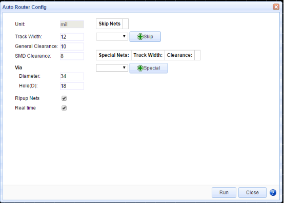
——Auto Router Config dialog.

——Effect of Auto Routing .
2、However , even the tool provides function to auto route, for most of the completed circuits or special circuits , you need to route it manually .
3、Use the PCB tools and the layers tools and use the track on the PCB Tool to connect every flying line .
4、Remember to check the DRC Routing Rule and then make the PCB Layout to make sure that it support power integrity .After you route the wire , change the size of Toplayer Silklayer .
5、Pour the Copper Area through the icon on the PCB tool. 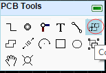
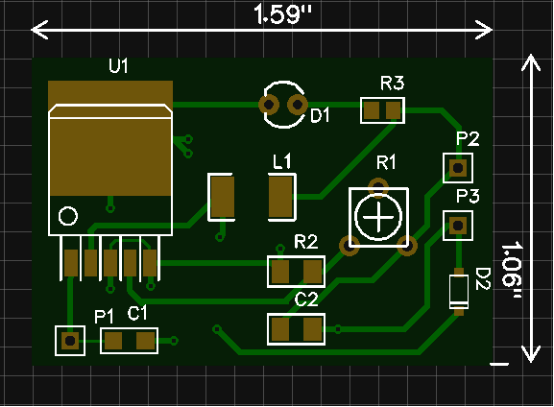
6、Press ”M” or click the “Dimension ”ICON on the PCB tool to measure the width and the length of the PCB board. 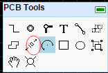

https://easyeda.com/GerryChen/LM2596_Module__Adjustable_DC_DC_Power_Converter_1_25V_35V_3A-4y4YgarJD
——Result of manual routing and measure the width or length of the circuit board .
7、Commonly we pour copper on the bottom layer as ground network ,pour the copper to the Top layer as the power network .
8、After you have route the PCB ,you could click the Designer Manager on the right hand side .
9、Then it will transfer to Properties .Click DRC Errors and Refresh .There are no DRC Errors in the PCB Layout .Click the components and nets , you could make every components or net bright. For example , choose C2 and The capacitor C2 will become bright .
10、Let us manually make an error . For Example , move MDC wire and there will be a big bright X and DRC Errors track2pad error.

Move the track to its previous location and then then big X and the DRC errors will disappear.
Once you have finished the PCB Layout , Click photo view to produce the Gerber file .
——PCB photo preview
11、If you want to order the PCB board ,Click the Fabrication Output icon in the Toolbar to order the PCB ,Then go to the Add to Cart Interface .
There are items like Numbers of Layers ,PCB Dimension Width and Height ,PCB Thickness ,PCBQTY,PCB Color,Surface Finish ,Copper Weight ,And Penalized PCB .
When you fill in all the Items above ,save it to cart. Then go the Network Payment Interface .
Delete the useless Gerber file .
Fill in your country ,your name ,your address ,your Post/Zip Code ,your Telephone ,Choose Delivery Method ,Network Payment Items ,and Click to send Request .
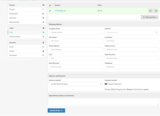
OK , then just wait for your PCB Order at home .
Top Comments
-

shabaz
-
Cancel
-
Vote Up
+1
Vote Down
-
-
Sign in to reply
-
More
-
Cancel
-

balearicdynamics
in reply to shabaz
-
Cancel
-
Vote Up
+3
Vote Down
-
-
Sign in to reply
-
More
-
Cancel
-

hadleywhite
in reply to balearicdynamics
-
Cancel
-
Vote Up
0
Vote Down
-
-
Sign in to reply
-
More
-
Cancel
Comment-

hadleywhite
in reply to balearicdynamics
-
Cancel
-
Vote Up
0
Vote Down
-
-
Sign in to reply
-
More
-
Cancel
Children