element14 Community
element14 Community
    Register Log In
  • Site
  • Search
  • Log In Register
  • Community Hub
    Community Hub
    • What's New on element14
    • Feedback and Support
    • Benefits of Membership
    • Personal Blogs
    • Members Area
    • Achievement Levels
  • Learn
    Learn
    • Ask an Expert
    • eBooks
    • element14 presents
    • Learning Center
    • Tech Spotlight
    • STEM Academy
    • Webinars, Training and Events
    • Learning Groups
  • Technologies
    Technologies
    • 3D Printing
    • FPGA
    • Industrial Automation
    • Internet of Things
    • Power & Energy
    • Sensors
    • Technology Groups
  • Challenges & Projects
    Challenges & Projects
    • Design Challenges
    • element14 presents Projects
    • Project14
    • Arduino Projects
    • Raspberry Pi Projects
    • Project Groups
  • Products
    Products
    • Arduino
    • Avnet Boards Community
    • Dev Tools
    • Manufacturers
    • Multicomp Pro
    • Product Groups
    • Raspberry Pi
    • RoadTests & Reviews
  • Store
    Store
    • Visit Your Store
    • Choose another store...
      • Europe
      •  Austria (German)
      •  Belgium (Dutch, French)
      •  Bulgaria (Bulgarian)
      •  Czech Republic (Czech)
      •  Denmark (Danish)
      •  Estonia (Estonian)
      •  Finland (Finnish)
      •  France (French)
      •  Germany (German)
      •  Hungary (Hungarian)
      •  Ireland
      •  Israel
      •  Italy (Italian)
      •  Latvia (Latvian)
      •  
      •  Lithuania (Lithuanian)
      •  Netherlands (Dutch)
      •  Norway (Norwegian)
      •  Poland (Polish)
      •  Portugal (Portuguese)
      •  Romania (Romanian)
      •  Russia (Russian)
      •  Slovakia (Slovak)
      •  Slovenia (Slovenian)
      •  Spain (Spanish)
      •  Sweden (Swedish)
      •  Switzerland(German, French)
      •  Turkey (Turkish)
      •  United Kingdom
      • Asia Pacific
      •  Australia
      •  China
      •  Hong Kong
      •  India
      •  Korea (Korean)
      •  Malaysia
      •  New Zealand
      •  Philippines
      •  Singapore
      •  Taiwan
      •  Thailand (Thai)
      • Americas
      •  Brazil (Portuguese)
      •  Canada
      •  Mexico (Spanish)
      •  United States
      Can't find the country/region you're looking for? Visit our export site or find a local distributor.
  • Translate
  • Profile
  • Settings
Open Source Hardware
  • Technologies
  • More
Open Source Hardware
Blog Kelvin (4-Wire) Milliohm Meter:  Version 1.3
  • Blog
  • Forum
  • Documents
  • Events
  • Polls
  • Members
  • Mentions
  • Sub-Groups
  • Tags
  • More
  • Cancel
  • New
Join Open Source Hardware to participate - click to join for free!
  • Share
  • More
  • Cancel
Group Actions
  • Group RSS
  • More
  • Cancel
Engagement
  • Author Author: fmilburn
  • Date Created: 24 Jan 2019 7:51 AM Date Created
  • Views 4257 views
  • Likes 13 likes
  • Comments 19 comments
  • kelvin measurement
  • op amp
  • 4 wire measurement
  • instrument op amp
  • milliohm measurement
  • milliohm
  • milliohm meter
Related
Recommended

Kelvin (4-Wire) Milliohm Meter:  Version 1.3

fmilburn
fmilburn
24 Jan 2019

This post documents Version 1.3 of an inexpensive but reasonably accurate meter for measuring resistance in the milliohm range. The development to date is documented in the links at the bottom of this post.  Version 1.3 contains numerous upgrades and suggestions from Shabaz, Gene Breniman, John Wiltrout, and Jon Clift to which I am indebted.  I intend to send off for new PCBs tomorrow evening and any comments in the meantime are greatly appreciated!  NOTE: This post was revised on 24 Jan 2019 to update the schematic and PCB screenshots per upgrades and comments from Shabaz.


Summary of Changes

  • Added biasing for VREF of the instrument op amp which improves reading of resistances around 1 milliohm
  • Added ability to add capacitance and / or diodes in front of instrument op amp
  • Moved trim pots to trim gain of operational amplifier - current sources are not trimmed
  • Modified arrangement of range switch
  • Changed PCB footprint to fit enclosure used by Shabaz
  • Added through hole 5V alternate input
  • Relocated on / off switch
  • Numerous other small improvements


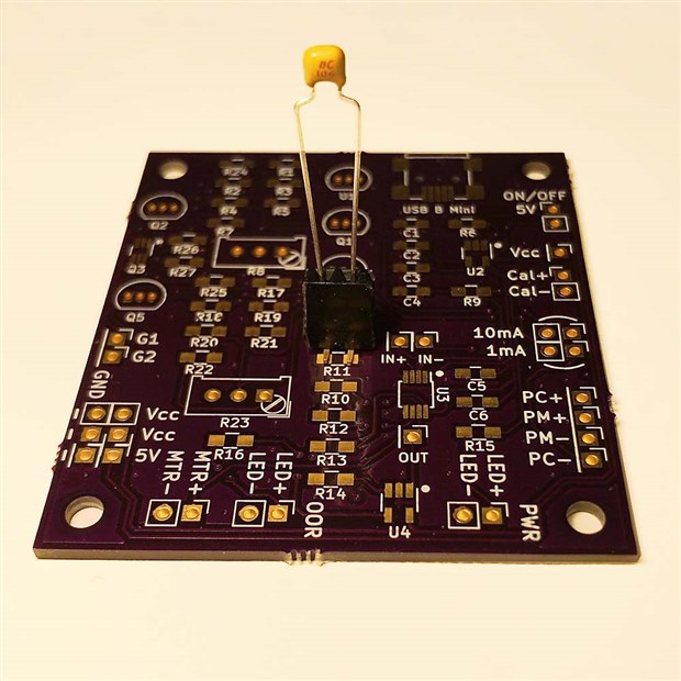
Development is a bit behind as I have been struggling to remove the one known bug - intermittent instability when measuring resistances below 20 milliohms.  I have been making modifications to the Version 1 PCB with flying leads to a breadboard.  This seems to introduce unwanted capacitance and perhaps other problems.  To address this and allow quick changing of components I have determined that I can bend the pins on duPont female sockets and solder them to an 0805 footprint.  Then insert passives as desired.  The black 2 pin socket is a bit hard to see but the concept is demonstrated in the mockup using the Version 1 PCB below.

image


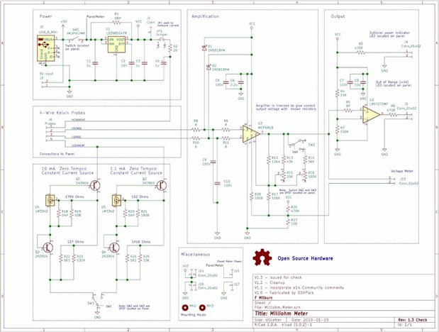
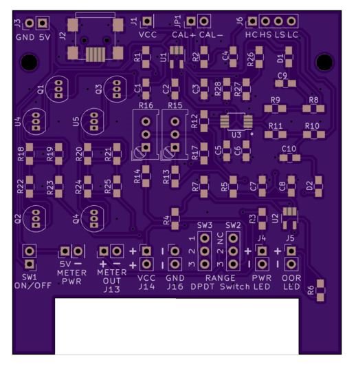
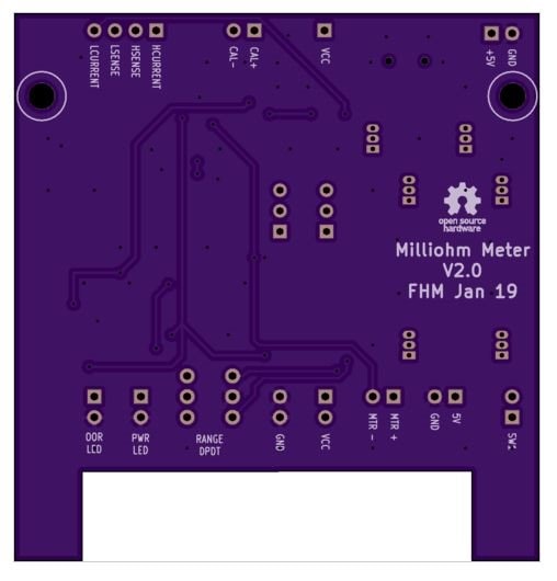
The new schematic and PCBs are shown below.


Schematic

The original schematic posted here was in error and has been replaced with the corrected version.

image

PCB

The original PCB screenshots posted here were replaced with a version that include an upgraded layout based on comments posted by Shabaz below.

image

image

image


As always, comments and suggestions are greatly appreciated!


Related Links

Building Frank's Milliohm Meter

Testing Current Sources for a Kelvin (4-Wire) Milliohm Meter

More on Current Sources and a Kelvin (4-Wire) Milliohm Meter

Even More on Current Sources and a Kelvin (4-Wire) Milliohm Meter

Working Prototype of a Kelvin (4-Wire) Milliohm Meter

PCB for a Kelvin (4-Wire) Milliohm Meter

  • Sign in to reply

Top Comments

  • shabaz
    shabaz over 6 years ago +10
    Hi Frank, Wow. I don't know how you manage keeping everything so neat on such a tiny PCB! I'll print it all off and do a review, in case I can spot anything. Just initially the red connection needs removing…
  • fmilburn
    fmilburn over 6 years ago in reply to shabaz +6
    Oops - I was in a hurry and that is an old / incorrect schematic which I should delete. I will repost with the correct one. Thanks and you have a keen eye. Great layout you have proposed. I need to design…
  • three-phase
    three-phase over 6 years ago +5
    Nice to see the good progress being made, look forward to seeing how the new version tests out. Kind regards
  • fmilburn
    fmilburn over 6 years ago in reply to geralds

    I agree these are all good suggestions Gerald. Currently I am hand soldering without a stencil and the spacing makes things much easier for me - especially since I have had to rework a few resistors wedged in close to larger components like the pots.  I keep thinking I need to set up a toaster oven and use stencils though...


    Frank

    • Cancel
    • Vote Up +1 Vote Down
    • Sign in to reply
    • More
    • Cancel
  • fmilburn
    fmilburn over 6 years ago in reply to geralds

    Hi Gerald,


    Thanks for taking the time to make the detailed and helpful comments. As you can tell, PCB design is not a core skill for me so the suggestions are much appreciated and I will revisit them should I respin the board. 


    I struggled with the star routing that you identified.  Would you consider it better to have a power bus for Vcc rather than the individual routing of wires?  These are the type of things I don’t have a good feeling for.

    • Cancel
    • Vote Up +1 Vote Down
    • Sign in to reply
    • More
    • Cancel
  • shabaz
    shabaz over 6 years ago in reply to geralds

    Hi Gerald!


    The changes you suggest are good, worth doing on any future revisions. Currently the PCB has all the surface-mount resistors spaced far apart, which is nice for hand construction for newcomers to SMD, so possibly makes the routing more of a challenge. Whereas for the person more equipped, their finer soldering tip and solder will handle even 25-50mil gap between the parts.

    • Cancel
    • Vote Up +1 Vote Down
    • Sign in to reply
    • More
    • Cancel
  • geralds
    geralds over 6 years ago in reply to shabaz

    Hi shabaz ,


    fine routing.


    What would you say?

    A bit arranging more closer the resistor group, then you can better going with VCC, straight in the middle through the IC.

    Then turning the C9 and C10 to 180° (to outside) placing to the R8 resp. R10, then switch C9 and D1 and placing D1 a bit closer to the IC.


    It was just an idea.


    Best Regards

    Gerald

    ---

    • Cancel
    • Vote Up +2 Vote Down
    • Sign in to reply
    • More
    • Cancel
  • geralds
    geralds over 6 years ago in reply to fmilburn

    Hi Frank fmilburn ,


    What would you say? - I would suggest to output a separate LDO as Vref for the Kelvin probe.

    e.g. I would say that you have 3 supply voltages:

    V_probe (eg 3.0 V, on the sink side you have the switch for the two currents, 10 mA, 1 mA)

    VCC (3.3V, slightly larger than the V_probe, rail / rail behavior)

    V_panelmeter (5V connected to the USB, before the LDOs)

    This is just an idea.

    I think the Kelvin jack can cause interference when replacing components. Then the OPAMPs may get into trouble.


    The PCB looks fine, but I have some ideas:

    image

    One thinking:

    If the tracks are not in an "correct" angle as well, then the polygon calculator (it calculates line by line horizontal) may calculate with wrong rounding values. You have in the polygon properties three values: width, spacing, isolating, with that the calculator works.

    This can cause that polygon edge in the middle of that track.


    Best Regards

    Gerald

    ---

    • Cancel
    • Vote Up +2 Vote Down
    • Sign in to reply
    • More
    • Cancel
>
element14 Community

element14 is the first online community specifically for engineers. Connect with your peers and get expert answers to your questions.

  • Members
  • Learn
  • Technologies
  • Challenges & Projects
  • Products
  • Store
  • About Us
  • Feedback & Support
  • FAQs
  • Terms of Use
  • Privacy Policy
  • Legal and Copyright Notices
  • Sitemap
  • Cookies

An Avnet Company © 2025 Premier Farnell Limited. All Rights Reserved.

Premier Farnell Ltd, registered in England and Wales (no 00876412), registered office: Farnell House, Forge Lane, Leeds LS12 2NE.

ICP 备案号 10220084.

Follow element14

  • X
  • Facebook
  • linkedin
  • YouTube