


Table of Contents
Introduction
Having used EAGLE CAD for several years, I had a set of projects, a select few of which I wanted to be able to import into KiCad and modify. Fortunately, KiCad has a built-in translator for this, but there are a few things to be aware of. The entire process can never be fully automated, because there isn’t a 1:1 mapping of features between the different CAD systems. This blog post covers some of the issues that may come up, and how to resolve them.
Note: The video is rather long (20 minutes) since there was much to cover. It's not a beginner video for people migrating from EAGLE. If you're a newcomer to KiCad, then perhaps this KiCad 6 quick start video could be more useful first (KiCad 6 information is compatible with KiCad 7). Incidentally, the example project used in the video is described here: Cyclops-1000: An Electronic Eye for Rotational Speed Measurement
Importing the project
The first part is very straightforward. Simply go to File->Import Non-KiCad Project->EAGLE Project and then select the EAGLE schematic file (the EAGLE PCB file will automatically be loaded). Select a destination folder for the converted KiCad project.
Once you do that, the schematic will be converted and then a window appears with EAGLE and KiCad layer names that need to be mapped.

Most of the layers can be auto-mapped, however some may need to be manually done. The trouble is, you might not know which layers need the manual work, until you click OK, and then you can’t go back in the workflow. It will be an iterative process, learning which layers you missed the first time round. In the example screenshot above, it was determined that the project happened to use the EAGLE Milling layer, so that needed to be manually mapped to the KiCad Edge.Cuts layer.
Click on OK, and you’ll see the PCB has now been converted too.
Enabling Schematic and PCB Updates
If you plan on editing the project in KiCad, then at some point, the Update PCB with changes made to the schematic icon (shown in the screenshot below) will need to be clicked. I encountered a problem with that! If that icon is clicked, the positions of all the component footprints are reset. They all move off the board! This is a major problem because there could be dozens or hundreds of components to re-position back to where they were before.
![]()
The only solution I know of is to initially not press that button! You can capture the position coordinates of every component footprint to a file, and then press that button, and then move the components back programmatically. Fortunately, this is straightforward using KiCad’s Python scripting feature.
To do that, save the ktools.py file into a folder, for instance C:/development/ktools :

Next, in the KiCad PCB editor window, click on Tools->Scripting Console to bring up a Python command prompt. Type the following (note: use forward-slashes for the path!):
import syssys.path.insert(1, "c:/development/ktools")import ktools as k
Now you can type the following command to print out a list of the coordinates of every component footprint on the board:
k.list_coords()

Although the printed list is useful information to browse through, this isn’t what is needed. Instead, the list_coords function can be called with a parameter to force the output to be in a Python format. Type:
k.list_coords(format='python')
Now you’ll see a load of output that is actually a Python program.

Copy-paste the output into a new file, called (say) myfix.py and save it into the same folder as the ktools.py file.
Now click on the Update PCB with changes made to the schematic icon, and you’ll see that the components move off their positions:

This is not a problem, since now they can be restored to their correct positions using the new myfix.py file. Type:
import myfixmyfix.move_items()
Everything should be back to normal! Now, you can press the Update PCB button at any time, and the components will remain where they should be.
Resolving PCB Problems
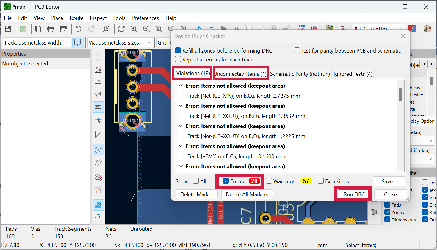
Click on Inspect->Design Rules Checker and run the DRC.
Zones (Copper planes)
You may find errors reported on copper planes (zones), and they are easy to fix by double-clicking on the zone to bring up the Properties window, and then setting the Clearance value to something sensible (for instance, 0.3 mm or more). Note that with KiCad 7, there is a Properties pane on the left side, so you don’t need to double-click for the Properties window, you could make the adjustment in the pane.

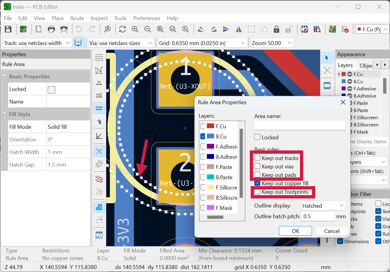
Rule Areas (Keepout regions)
You may find that EAGLE keepout areas, intended to prevent copper pours, may have defaulted in KiCad to keeping out pads and traces too. This is easy to fix by double-clicking on the keepout area, and unchecking things:
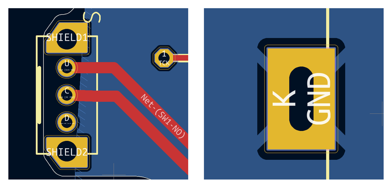
Component Footprints
The screenshots below show what might also be typical problems, regarding component footprints. In EAGLE, shaped pads are really just shaped elements and milling outlines stacked on top of pads, whereas KiCad natively supports pads and slotted cut-outs all integrated into the single pad element.

The best thing to do is to edit the component, get rid of the EAGLE elements and fix it properly, using proper KiCad pad techniques (in particular, the Pad Edit Mode, invoked by pressing Ctrl-E. If you’ve not used this function before, check out the video above). The end result will be decent-looking pads, that were not ever achievable with EAGLE!:
Resolving Schematic Problems
There are a couple of minor issues that could occur with EAGLE imported schematics.
Text Sizes
If you decide to modify the schematic, there is a possibility that KiCad component symbols will have a different text size compared to the imported EAGLE text. The screenshot below shows that the EAGLE imported resistor R1 has slightly larger text than the newly added resistor R9.

An easy way to solve this is to perform a text search-and-replace in the KiCad schematic file. For instance, for the example schematic in the screenshot above, I replaced the text 1.778 1.5113 with 1.27 1.27 and that resolved it.

Drawing Frame
If the KiCad file has a drawing frame, then you’ll notice an irritating problem in the KiCad schematic. If you try to select any component, it is very easy for the frame to get selected instead since it surrounds the entire schematic area.
I don’t know of a good solution, except to delete the frame. If you know of a better solution, please let me know!
Summary
If there are legacy EAGLE projects that you would really like to edit within KiCad, then it is possible to use the built-in EAGLE import capability, however, you should expect to have to make some changes manually. You may need to use a Python script and also text search-and-replace, but that is not difficult.
In some cases, there may not be much extra that needs to be done, but it depends on what EAGLE features were used in the project. In particular, EAGLE has a very different (and awkward) approach for complex component footprints, which is best resolved by re-implementing parts of the footprints.
Thanks for reading!


