element14 Community
element14 Community
    Register Log In
  • Site
  • Search
  • Log In Register
  • About Us
  • Community Hub
    Community Hub
    • What's New on element14
    • Feedback and Support
    • Benefits of Membership
    • Personal Blogs
    • Members Area
    • Achievement Levels
  • Learn
    Learn
    • Ask an Expert
    • eBooks
    • element14 presents
    • Learning Center
    • Tech Spotlight
    • STEM Academy
    • Webinars, Training and Events
    • Learning Groups
  • Technologies
    Technologies
    • 3D Printing
    • FPGA
    • Industrial Automation
    • Internet of Things
    • Power & Energy
    • Sensors
    • Technology Groups
  • Challenges & Projects
    Challenges & Projects
    • Design Challenges
    • element14 presents Projects
    • Project14
    • Arduino Projects
    • Raspberry Pi Projects
    • Project Groups
  • Products
    Products
    • Arduino
    • Avnet Boards Community
    • Dev Tools
    • Manufacturers
    • Multicomp Pro
    • Product Groups
    • Raspberry Pi
    • RoadTests & Reviews
  • Store
    Store
    • Visit Your Store
    • Choose another store...
      • Europe
      •  Austria (German)
      •  Belgium (Dutch, French)
      •  Bulgaria (Bulgarian)
      •  Czech Republic (Czech)
      •  Denmark (Danish)
      •  Estonia (Estonian)
      •  Finland (Finnish)
      •  France (French)
      •  Germany (German)
      •  Hungary (Hungarian)
      •  Ireland
      •  Israel
      •  Italy (Italian)
      •  Latvia (Latvian)
      •  
      •  Lithuania (Lithuanian)
      •  Netherlands (Dutch)
      •  Norway (Norwegian)
      •  Poland (Polish)
      •  Portugal (Portuguese)
      •  Romania (Romanian)
      •  Russia (Russian)
      •  Slovakia (Slovak)
      •  Slovenia (Slovenian)
      •  Spain (Spanish)
      •  Sweden (Swedish)
      •  Switzerland(German, French)
      •  Turkey (Turkish)
      •  United Kingdom
      • Asia Pacific
      •  Australia
      •  China
      •  Hong Kong
      •  India
      •  Korea (Korean)
      •  Malaysia
      •  New Zealand
      •  Philippines
      •  Singapore
      •  Taiwan
      •  Thailand (Thai)
      • Americas
      •  Brazil (Portuguese)
      •  Canada
      •  Mexico (Spanish)
      •  United States
      Can't find the country/region you're looking for? Visit our export site or find a local distributor.
  • Translate
  • Profile
  • Settings
Open Source Hardware
  • Technologies
  • More
Open Source Hardware
Forum PCB Stencil Printer - Alignment discussion
  • Blog
  • Forum
  • Documents
  • Events
  • Polls
  • Members
  • Mentions
  • Sub-Groups
  • Tags
  • More
  • Cancel
  • New
Join Open Source Hardware to participate - click to join for free!
Actions
  • Share
  • More
  • Cancel
Forum Thread Details
  • Replies 29 replies
  • Subscribers 312 subscribers
  • Views 5098 views
  • Users 0 members are here
  • pcb_prototyping
  • stencil printer
  • smt
  • pcb_stencil
  • smt stencil
Related

PCB Stencil Printer - Alignment discussion

shabaz
shabaz over 8 years ago

Hi,


For prototyping, I've noticed stencils are quite low-cost nowadays, which is fantastic.

For those unfamiliar with the process, they are used to apply solder paste to the correct areas on a PCB prior to component placement and reflow soldering.

The basic principle can be seen in this screenshot from a sparkfun stencilling video:

image

In that video, the PCB is secured in the XY plane using scrap PCBs that are temporarily taped to the desk, and then a laser-cut mylar template (it has laser-cut apertures which correspond to the pads on the PCB where solder paste is needed) is held in place (aligned by eye) and then paste is applied using a squeegee.

So, that's the fundamentals of the process, but in practice it may need some refinement for certain use-cases.


I'd like to use low-cost stencils (actually steel sheet stencils are low-cost nowadays, the Sparkfun video is six years old) but for perhaps half a dozen boards or more; in other words not production volumes, but "a few to a couple of dozen prototypes" volumes, and then discarding the stencil. Furthermore, nowadays tiny packages are very common for hobbyists to use too, so clamping of the stencil by hand isn't feasible. Perhaps alignment even needs to be inspected under a magnifier/microscope unless there are registration holes or pegs that can be used to obtain some accuracy without having to align by eye each time. How much accuracy is needed? I think an error around 0.1mm may be a suitable limit, because there are components that have 0.5mm or 0.4mm pitch and an offset of 0.1mm could mean that 25% less solder paste is on the pad.


There are many other parts to the process that could be refined too, but for now I wanted to focus on the the alignment/clamping topic.


The commercial solution is a stencil printing machine; for low volume prototyping there are manual versions of such machines. The way they work is that the stencil has a metal frame around it, and this is clamped/fitted into the machine on a hinge. The frame is lowered to do the pasting, then the frame is raised on the hinge to take out the pasted PCB and  insert the next PCB.


However, framed stencils cost more. It is possible to self-frame, but this requires a stencil with lots of space around it. The squeegee may be 100mm wide or more, but hobby PCBs are often smaller than 100mm. A low-cost stencil may only be 20mm wider all around.

Adding a custom frame to a low-cost stencil is therefore hard when the squeegee itself could be of a similar size to the stencil.


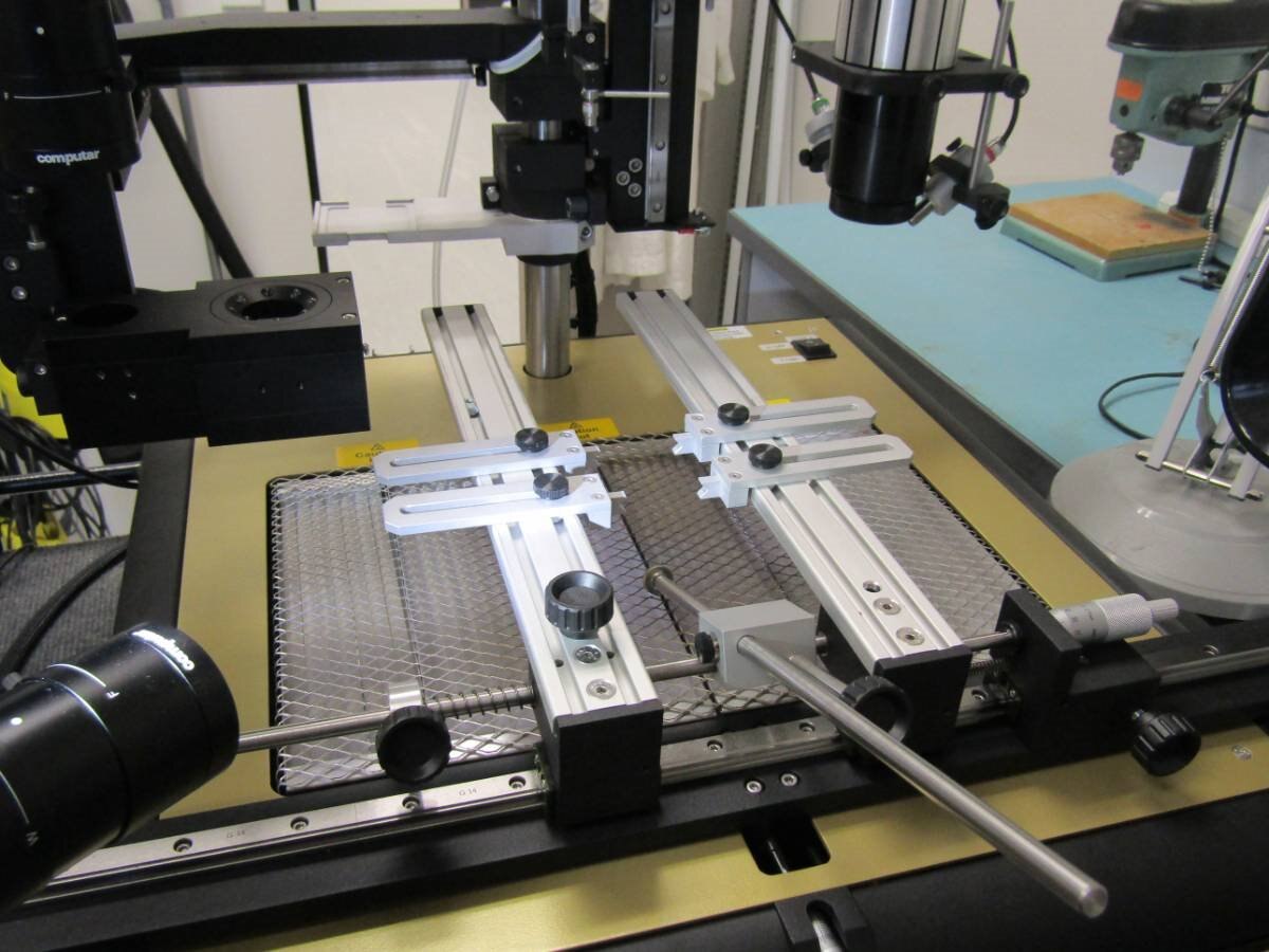
I tried to think of a way to solve this issue. The diagram here shows the current thought process.

image


Basically the PCB would fit on a raised platform that is attached to a base. The raised platform could be swapped out for different PCB projects or drilled with more peg positions or have straight edges for aligning the PCB into a repeatable XY plane position. The height of the raised platform would be fixed for a certain PCB thickness but could be modified with some shim if needed. The raised platform could be screwed to the base from the underside. The base and raised platform would probably be  constructed from aluminium sheet.


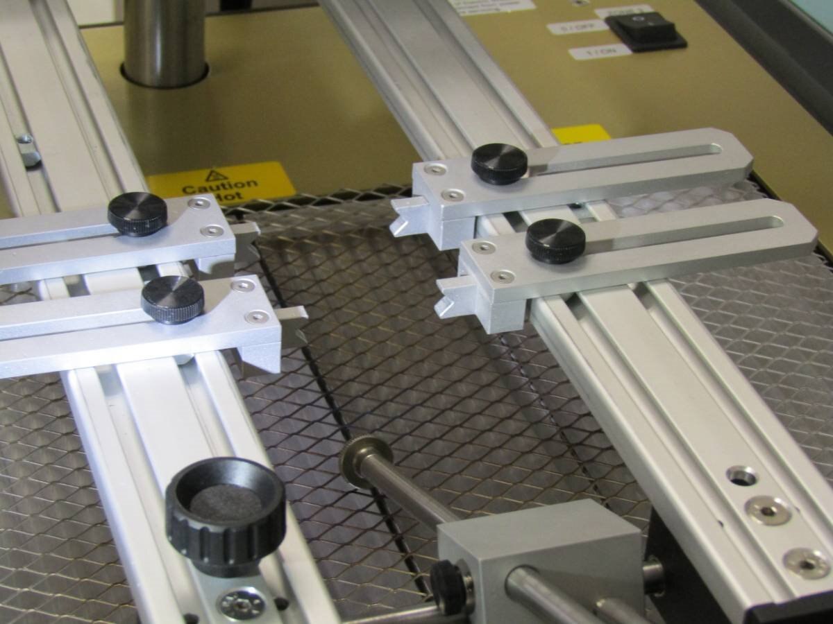
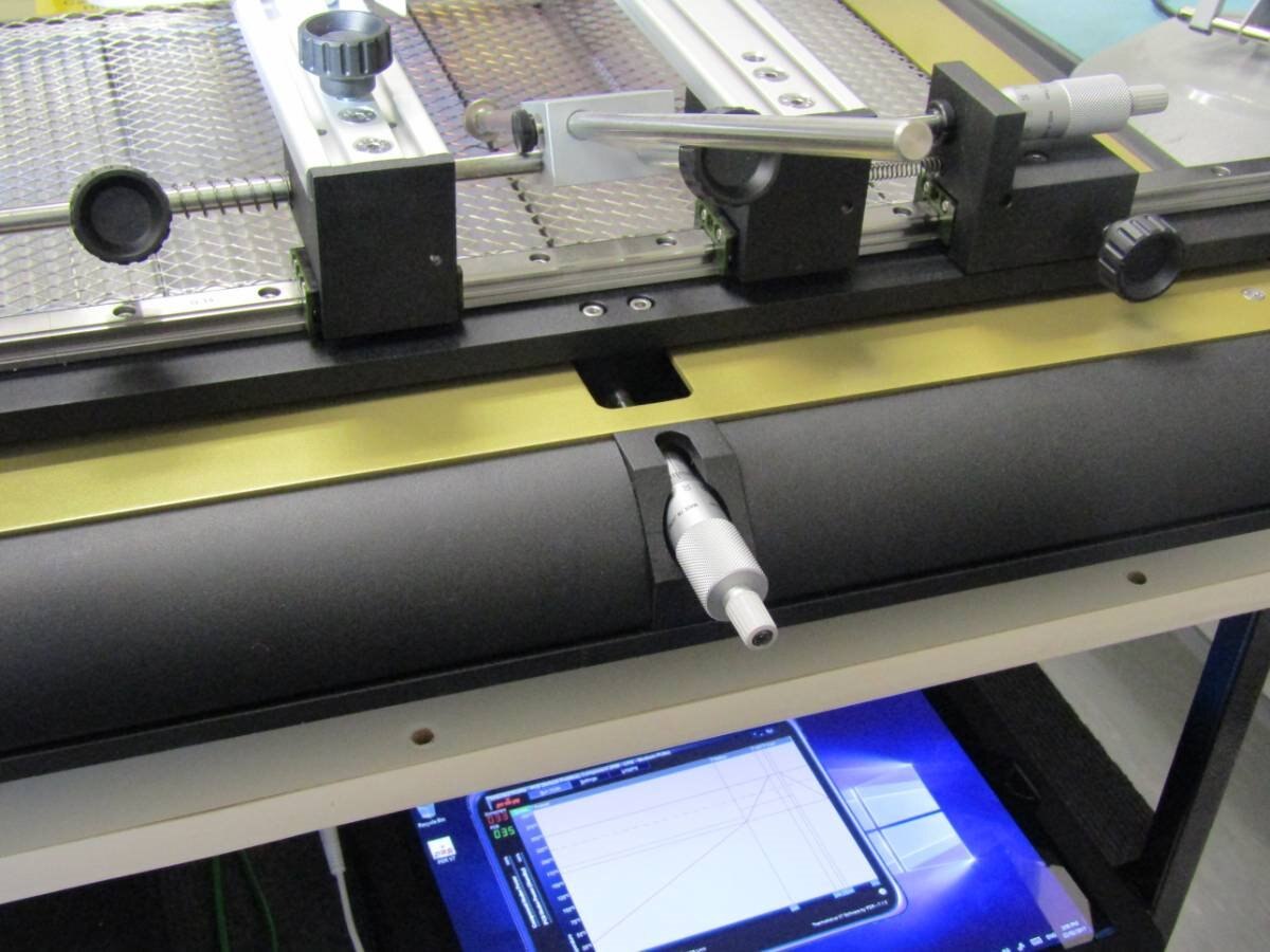
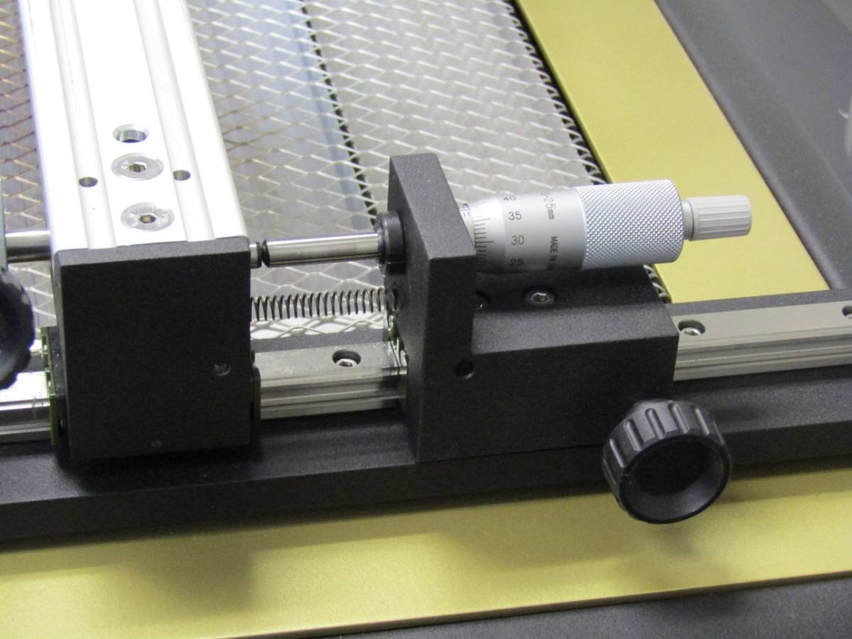
The stencil sheet would be clamped on one edge between two blocks shown in blue. This could be achieved using screws or winged nuts. The precise alignment would come from loosening the screws, moving the sheet manually and then tightening it.  If the stencil has 5mm holes then the clamping could be done with 3 or 4mm screws as an example, to provide for adjustment.


The underside of the lower clamp block would have a couple of pegs that would fit into the base. These would allow for repeatable accuracy with insertion and removal of the clamp from the base. After a board has been pasted, the stencil and base would be carefully lifted and put to one side while the PCB is removed and a new PCB is inserted. Then the stencil/clamp would be placed back onto the base, and the alignment should not have changed.

Although commercial screen printing machines use a hinged action for lifting the stencil, I'm wondering for small boards if this is needed or not; perhaps it is just as easy to lift up the stencil from the unclamped end slightly with a ruler for example, and then lift off the clamp from the base. I don't mind if I need to go carefully because I'm not doing production volumes; I can afford to take some extra minutes of care per board.


I already have some ideas about how I will go about this which I'll jot down as I experiment (and eventually write it up in a blog post so that it can be replicated), and I'm curious if others were to do this, what tips/suggestions would you have?

I'm still researching some materials and methods for assembly. For peg alignment I'd clamp the materials together and drill right through, so that the base and clamp are all drilled identically, unless I can find off-the-shelf pegs and sockets that I could incorporate into the design.

I might use bits of optical breadboards etc to save having to drill too many holes precisely.


Many thanks!


Message was edited by: shabaz (Corrected the diagram to indicate the scrap PCBs to prevent damage to the stencil on edges)

  • Sign in to reply
  • Cancel

Top Replies

  • Problemchild
    Problemchild over 8 years ago in reply to shabaz +3
    Hi Shabaz it's quite standard to cut Mylar with a laser. I've not cut actual Mylar but it's only a stretched Polyester film and I've cut them. I think stencils based on Mylar have a reduced life of say…
  • shabaz
    shabaz over 8 years ago +3
    Just a mini progress report.. Currently I'm exploring options..! I will chop the long aluminium rails tomorrow, so that the size of the entire thing is about 280x320mm. If I don't get decent stability…
  • shabaz
    shabaz over 8 years ago +3
    I thought it would be worth sharing photos of what is possible using the 'tape hinge' method (i.e. where sticky tape is used to secure a stencil along one edge, much like this photo from the Internet)…
Parents
  • shabaz
    shabaz over 8 years ago

    Just a mini progress report.. Currently I'm exploring options..!

    I will chop the long aluminium rails tomorrow, so that the size of the entire thing is about 280x320mm.

    If I don't get decent stability from the rails as a base, then I'll throw them out and replace with a frame made of beams.

    The rails are easier to try quickly first, because all the punched holes mean I don't need to drill any holes in them at all!

    The aluminium bars on the lower-right of the photo are going to be tapped for the positioning screws that will push the floating platform into place.


    image

    • Cancel
    • Vote Up +3 Vote Down
    • Sign in to reply
    • Cancel
  • Problemchild
    Problemchild over 8 years ago in reply to shabaz

    I'm liking this a lot Shabaz. I'll be very interested to see how this works out !

    • Cancel
    • Vote Up +1 Vote Down
    • Sign in to reply
    • Cancel
  • mcb1
    mcb1 over 8 years ago in reply to Problemchild

    shabaz

    I took some extra pictures to show the holder and the adjusters on the PDR E3 here First Steps - Intel Edison Repair


      imageimage


    imageimage


    Looking at the verniers, it seems they might originate from a micrometer.


    mark

    • Cancel
    • Vote Up +1 Vote Down
    • Sign in to reply
    • Cancel
  • shabaz
    shabaz over 8 years ago in reply to mcb1

    Hey Mark,


    That's a nice reminder, how easy it is to get verniers from micrometers. When I last looked at some super-cheap Draper ones, it is easy to undo the screw and remove the 'C' portion.

    Excellent idea, I've already purchased the 100th-inch-pitch screws but the micrometer idea is better.

    I've ditched the alu rails, they were not folded completely square, and instead will just use the aluminium slab I had for the the base, it is about 300x250mm and quarter inch thick, so quite heavy but at least it is flat.

    The proper extruded rails and steel rods on your PDR E3 are nice, that would have been lighter but I'll just use what I have for now.

    I've been stuck at a trade show all week, so work resumes on this project next week!

    • Cancel
    • Vote Up +1 Vote Down
    • Sign in to reply
    • Cancel
Reply
  • shabaz
    shabaz over 8 years ago in reply to mcb1

    Hey Mark,


    That's a nice reminder, how easy it is to get verniers from micrometers. When I last looked at some super-cheap Draper ones, it is easy to undo the screw and remove the 'C' portion.

    Excellent idea, I've already purchased the 100th-inch-pitch screws but the micrometer idea is better.

    I've ditched the alu rails, they were not folded completely square, and instead will just use the aluminium slab I had for the the base, it is about 300x250mm and quarter inch thick, so quite heavy but at least it is flat.

    The proper extruded rails and steel rods on your PDR E3 are nice, that would have been lighter but I'll just use what I have for now.

    I've been stuck at a trade show all week, so work resumes on this project next week!

    • Cancel
    • Vote Up +1 Vote Down
    • Sign in to reply
    • Cancel
Children
No Data
element14 Community

element14 is the first online community specifically for engineers. Connect with your peers and get expert answers to your questions.

  • Members
  • Learn
  • Technologies
  • Challenges & Projects
  • Products
  • Store
  • About Us
  • Feedback & Support
  • FAQs
  • Terms of Use
  • Privacy Policy
  • Legal and Copyright Notices
  • Sitemap
  • Cookies

An Avnet Company © 2025 Premier Farnell Limited. All Rights Reserved.

Premier Farnell Ltd, registered in England and Wales (no 00876412), registered office: Farnell House, Forge Lane, Leeds LS12 2NE.

ICP 备案号 10220084.

Follow element14

  • X
  • Facebook
  • linkedin
  • YouTube