

.jpg)

Table of Contents
(Test: Edited at 01:26 GMT 14th Dec 2022)
Introduction
I’m interested in finding ways to provide phone and laptop power during times when mains power could be absent. Since many phones and laptops have USB Type C (also known as USB-C) connections, this could be a great way to get power into them, without having to use mains voltages connected to AC mains power bricks/chargers.
The technology that gets a lot of power over USB-C, is called USB-C Power Delivery (PD). It is possible to use this technology to connect (say) a car battery to the phone or laptop. USB-C PD “sink” technology is used by the phone/laptop end, to negotiate with the USB-C PD “source” end, to decide on what voltage should be sent across the USB cable. It's easier to see how it approximately works and what this project is about, by looking at the overview diagram below.

I don't know a lot about USB-C, so this project will help me discover a bit more about a small aspect of it. If you're interested to learn about USB-C too, then it would be great to simultaneously build this partial project and test it out : ) Some more areas of USB-C PD are discussed here: USB Type-C and Power Delivery: Any Interest?
For this project, I decided to build a circuit that can connect to a large battery at one end, and expose a USB-C connector at the other end of the circuit, that will connect to the phone or laptop. This should provide many hours of device operation during a mains power outage. The power output might reach 100W (but I’m not sure), and the project is very low cost (about £15-20 parts cost), and several of the boards could be constructed and used simultaneously to power multiple devices.
Although most car batteries offer about 12V, this project actually requires about 24V (it can support up to 32V) due to only using easily-obtainable components that are currently in stock. To use this project two 12V car batteries could be placed in series, or alternatively, the design can be preceded with a separate DC-DC converter board to step up 12V to 24V. It wouldn’t be as efficient, however. Still, for my first USB-C PD Source prototype, I am OK with the input voltage requirement, and I can always upgrade the DC-DC converter portion later if the 24V need becomes very inconvenient once I further refine requirements, and once I understand USB-C PD technology better.
Circuit Design
1. Power Delivery (PD) Source Function
The MP5031 Power Delivery Controller chip was used because it contains the “Source” functionality.
 (Image source: MPS website)
The MP5031 chip can advertise different power capabilities and can send control signals to the DC-DC converter to adjust the voltage output.
There is an I2C interface, but I believe (not 100% sure) it won’t be needed for a basic configuration. The I2C connections will be broken out to pin headers, in case the configuration needs to be set. Care would be needed because nearly all configuration registers are only one-time programmable (OTP). Incidentally from the block diagram, it can be seen that the MP5031 also supports USB 2.0 Battery Charging negotiation, known as BCS 1.2, in case a USB 2.0 device is connected.
2. DC-DC Converter
The MP2491C DC-DC converter chip was used. It has internal MOSFET switching to simplify the design a bit. It also has a small secondary output, 5V, that can be used to power a small amount of external circuitry.
A couple of voltage-select pins, VSEL1 and VSEL2, are used by the PD Source chip to control the DC-DC converter output. The two pins will adjust the reference voltage used in the feedback loop. Five different voltages are possible (5, 9, 12, 15, and 20 V), depending on if the VSEL pins are at 0V, 5V, or 2.5V.
The Power Good (PG) pin changes state while the output is unsettled.
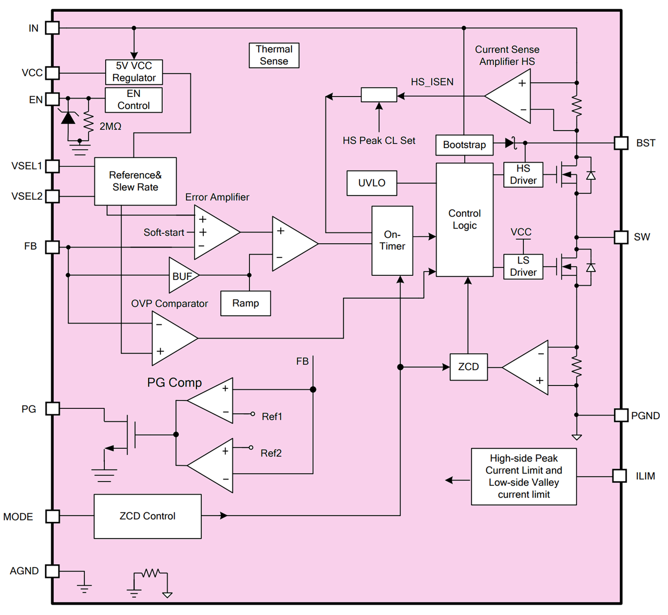 Image source: MPS website
The overall combined circuit diagram is shown below (there is a more readable PDF version attached to the blog post further below).

Printed Circuit Board (PCB) and Enclosure
The project is supposed to be low-cost, and it is designed to fit a cheap aluminium extrusion, known as E-Case A, and aluminium end-plates and screws can be ordered separately, or PCB end-plates could be designed so that no custom drilling is required.
 Image source: Lincoln Binns website
Alternatively, perhaps a 3D-printed enclosure would be possible (I don’t have a 3D printer, so I didn’t investigate this). The board size is 40 x 55 mm.
The 24V DC input uses a Molex Mini-Fit Jr board-mount connector part code 172648-0102 or wires could be soldered in the holes if a different connection is required.
All parts are large where possible, and hand-solderable. The MP5031 and MP2491C parts are small, unfortunately, but still manageable.

Inner layers:

The zip file is attached to this blog post, ready for sending to a PCB factory. The cost for five boards is about $7 + shipping, depending on which PCB factory you order it from. Incidentally, I have not built or ordered the board yet, so there may be faults in the design.
The bill of materials is attached. The finished board should look (almost) like this:

Summary
A USB Power Delivery Source IC was combined with a DC-DC converter chip, to be able to supply five different voltages and support up to 100W. The actual power output will partially be dependent on the board layout, so it’s not guaranteed currently. The project is very low cost (under £20) and all parts are currently in-stock. I’m hoping that this project will help a bit during any potential mains power outages, to continue operating computing equipment. Even if it doesn’t, it will be a good experience learning about USB-C power delivery.
Thanks for reading!
export_usb_c_power_supply_gerbers_v1.zip

