element14 Community
element14 Community
    Register Log In
  • Site
  • Search
  • Log In Register
  • Community Hub
    Community Hub
    • What's New on element14
    • Feedback and Support
    • Benefits of Membership
    • Personal Blogs
    • Members Area
    • Achievement Levels
  • Learn
    Learn
    • Ask an Expert
    • eBooks
    • element14 presents
    • Learning Center
    • Tech Spotlight
    • STEM Academy
    • Webinars, Training and Events
    • Learning Groups
  • Technologies
    Technologies
    • 3D Printing
    • FPGA
    • Industrial Automation
    • Internet of Things
    • Power & Energy
    • Sensors
    • Technology Groups
  • Challenges & Projects
    Challenges & Projects
    • Design Challenges
    • element14 presents Projects
    • Project14
    • Arduino Projects
    • Raspberry Pi Projects
    • Project Groups
  • Products
    Products
    • Arduino
    • Avnet Boards Community
    • Dev Tools
    • Manufacturers
    • Multicomp Pro
    • Product Groups
    • Raspberry Pi
    • RoadTests & Reviews
  • Store
    Store
    • Visit Your Store
    • Choose another store...
      • Europe
      •  Austria (German)
      •  Belgium (Dutch, French)
      •  Bulgaria (Bulgarian)
      •  Czech Republic (Czech)
      •  Denmark (Danish)
      •  Estonia (Estonian)
      •  Finland (Finnish)
      •  France (French)
      •  Germany (German)
      •  Hungary (Hungarian)
      •  Ireland
      •  Israel
      •  Italy (Italian)
      •  Latvia (Latvian)
      •  
      •  Lithuania (Lithuanian)
      •  Netherlands (Dutch)
      •  Norway (Norwegian)
      •  Poland (Polish)
      •  Portugal (Portuguese)
      •  Romania (Romanian)
      •  Russia (Russian)
      •  Slovakia (Slovak)
      •  Slovenia (Slovenian)
      •  Spain (Spanish)
      •  Sweden (Swedish)
      •  Switzerland(German, French)
      •  Turkey (Turkish)
      •  United Kingdom
      • Asia Pacific
      •  Australia
      •  China
      •  Hong Kong
      •  India
      •  Korea (Korean)
      •  Malaysia
      •  New Zealand
      •  Philippines
      •  Singapore
      •  Taiwan
      •  Thailand (Thai)
      • Americas
      •  Brazil (Portuguese)
      •  Canada
      •  Mexico (Spanish)
      •  United States
      Can't find the country/region you're looking for? Visit our export site or find a local distributor.
  • Translate
  • Profile
  • Settings
Power & Energy
  • Technologies
  • More
Power & Energy
Blog 100W USB Type-C Power Delivery Source: Getting Started
  • Blog
  • Forum
  • Quiz
  • Documents
  • Polls
  • Events
  • Mentions
  • Sub-Groups
  • Tags
  • More
  • Cancel
  • New
  • Share
  • More
  • Cancel
Group Actions
  • Group RSS
  • More
  • Cancel
EMI-Reduction-Techniques
Engagement
  • Author Author: shabaz
  • Date Created: 13 Dec 2022 2:08 AM Date Created
  • Views 15286 views
  • Likes 14 likes
  • Comments 15 comments
  • power delivery
  • monolithic power
  • usb type-c
  • usb-c
  • usb-c connector
  • usb pd
  • mps
Related
Recommended

100W USB Type-C Power Delivery Source: Getting Started

shabaz
shabaz
13 Dec 2022

Table of Contents

  • Introduction
  • Circuit Design
    • 1. Power Delivery (PD) Source Function
    • 2. DC-DC Converter
  • Printed Circuit Board (PCB) and Enclosure
  • Summary

(Test: Edited at 01:26 GMT 14th Dec 2022)

Introduction

I’m interested in finding ways to provide phone and laptop power during times when mains power could be absent. Since many phones and laptops have USB Type C (also known as USB-C) connections, this could be a great way to get power into them, without having to use mains voltages connected to AC mains power bricks/chargers.

The technology that gets a lot of power over USB-C, is called USB-C Power Delivery (PD). It is possible to use this technology to connect (say) a car battery to the phone or laptop. USB-C PD “sink” technology is used by the phone/laptop end, to negotiate with the USB-C PD “source” end, to decide on what voltage should be sent across the USB cable. It's easier to see how it approximately works and what this project is about, by looking at the overview diagram below.

image

I don't know a lot about USB-C, so this project will help me discover a bit more about a small aspect of it. If you're interested to learn about USB-C too, then it would be great to simultaneously build this partial project and test it out : ) Some more areas of USB-C PD are discussed here:  USB Type-C and Power Delivery: Any Interest?  

For this project, I decided to build a circuit that can connect to a large battery at one end, and expose a USB-C connector at the other end of the circuit, that will connect to the phone or laptop. This should provide many hours of device operation during a mains power outage. The power output might reach 100W (but I’m not sure), and the project is very low cost (about £15-20 parts cost), and several of the boards could be constructed and used simultaneously to power multiple devices.

Although most car batteries offer about 12V, this project actually requires about 24V (it can support up to 32V) due to only using easily-obtainable components that are currently in stock. To use this project two 12V car batteries could be placed in series, or alternatively, the design can be preceded with a separate DC-DC converter board to step up 12V to 24V. It wouldn’t be as efficient, however. Still, for my first USB-C PD Source prototype, I am OK with the input voltage requirement, and I can always upgrade the DC-DC converter portion later if the 24V need becomes very inconvenient once I further refine requirements, and once I understand USB-C PD technology better.

Circuit Design

1. Power Delivery (PD) Source Function

The MP5031 Power Delivery Controller chip was used because it contains the “Source” functionality.

image(Image source: MPS website)


The MP5031 chip can advertise different power capabilities and can send control signals to the DC-DC converter to adjust the voltage output.

There is an I2C interface, but I believe (not 100% sure) it won’t be needed for a basic configuration. The I2C connections will be broken out to pin headers, in case the configuration needs to be set. Care would be needed because nearly all configuration registers are only one-time programmable (OTP). Incidentally from the block diagram, it can be seen that the MP5031 also supports USB 2.0 Battery Charging negotiation, known as BCS 1.2, in case a USB 2.0 device is connected.

2. DC-DC Converter

The MP2491C DC-DC converter chip was used. It has internal MOSFET switching to simplify the design a bit. It also has a small secondary output, 5V, that can be used to power a small amount of external circuitry.

A couple of voltage-select pins, VSEL1 and VSEL2, are used by the PD Source chip to control the DC-DC converter output. The two pins will adjust the reference voltage used in the feedback loop. Five different voltages are possible (5, 9, 12, 15, and 20 V), depending on if the VSEL pins are at 0V, 5V, or 2.5V.

The Power Good (PG) pin changes state while the output is unsettled.
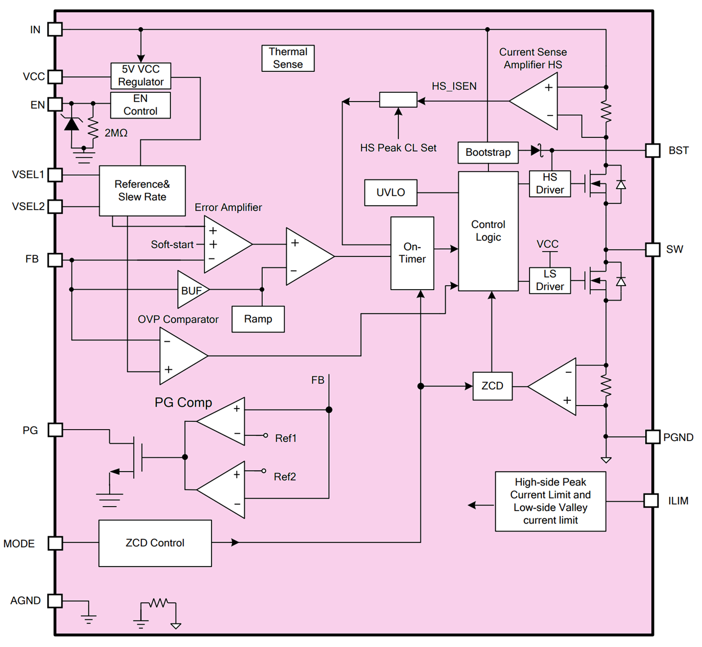
imageImage source: MPS website


The overall combined circuit diagram is shown below (there is a more readable PDF version attached to the blog post further below).

image

Printed Circuit Board (PCB) and Enclosure

The project is supposed to be low-cost, and it is designed to fit a cheap aluminium extrusion, known as E-Case A, and aluminium end-plates and screws can be ordered separately, or PCB end-plates could be designed so that no custom drilling is required.

imageImage source: Lincoln Binns website


Alternatively, perhaps a 3D-printed enclosure would be possible (I don’t have a 3D printer, so I didn’t investigate this). The board size is 40 x 55 mm.

The 24V DC input uses a Molex Mini-Fit Jr board-mount connector part code 172648-0102 or wires could be soldered in the holes if a different connection is required.

All parts are large where possible, and hand-solderable. The MP5031 and MP2491C parts are small, unfortunately, but still manageable.

image

Inner layers:

image

The zip file is attached to this blog post, ready for sending to a PCB factory. The cost for five boards is about $7 + shipping, depending on which PCB factory you order it from. Incidentally, I have not built or ordered the board yet, so there may be faults in the design.

The bill of materials is attached. The finished board should look (almost) like this:

image

Summary

A USB Power Delivery Source IC was combined with a DC-DC converter chip, to be able to supply five different voltages and support up to 100W. The actual power output will partially be dependent on the board layout, so it’s not guaranteed currently. The project is very low cost (under £20) and all parts are currently in-stock. I’m hoping that this project will help a bit during any potential mains power outages, to continue operating computing equipment. Even if it doesn’t, it will be a good experience learning about USB-C power delivery.

Thanks for reading!

export_usb_c_power_supply_gerbers_v1.zip

  • Sign in to reply
  • shabaz
    shabaz over 2 years ago in reply to Jan Cumps

    I too was concerned about soldering the inductor. However, just noticed a very neat feature in KiCAD that could be a semi-fix.

    (In the screenshot below, the exposed copper pads for the inductor are 4mm wide, and 5mm tall, just for an idea of scale).

    The left and right pads can be set to totally different thermal relief schemes, so I'm thinking, on the left side, I could leave off the thermal relief, since the copper is only on one layer. On the right side, the copper is on two layers, both with 2 oz copper, so there's around double the copper in that area, and I could use some thermal relief benefits in that side.

    All a bit of a guess though, if the two sides would reflow at the same time! 

    image

    • Cancel
    • Vote Up 0 Vote Down
    • Sign in to reply
    • More
    • Cancel
  • Jan Cumps
    Jan Cumps over 2 years ago in reply to Jan Cumps

    image

    • Cancel
    • Vote Up 0 Vote Down
    • Sign in to reply
    • More
    • Cancel
  • Jan Cumps
    Jan Cumps over 2 years ago in reply to shabaz

    I've worked with similar footprint, a TI LMG5200 GaN half-bridge.

    All-in-all, easier to solder with hot air than those cubic inductors with 2 large pads on the bottom, and lots of temperature-fighting mass.

    • Cancel
    • Vote Up 0 Vote Down
    • Sign in to reply
    • More
    • Cancel
  • shabaz
    shabaz over 2 years ago

    Really impressed with KiCad. It's possible to export the 3D file, and then import it into FreeCAD. 

    image

    I wanted to see what would happen if two boards were inserted, and I tried that, and could see that the large electrolytic would clash with the DC input connector, if the boards were placed face-to-face.

    It was hard though, because I can barely use FreeCAD. I had little idea what I was doing. It seems to be quite a difficult application to learn without any tutorial/video.

    (Anyway, I'm not going to spend time right now learning it, it's not that important currently, it will be something for the future).

    It's been a year since I started using KiCAD, and I now like it a lot, despite some things being clunky, a lot of things are great. I donated a bit of money to them today, since they are on a funding drive again.

    • Cancel
    • Vote Up 0 Vote Down
    • Sign in to reply
    • More
    • Cancel
  • shabaz
    shabaz over 2 years ago in reply to wolfgangfriedrich

    Hi Wolfgang,

    Thanks for the feedback! 

    I had a look, and figured a way to get the NTC close to the IC, so I went ahead and did it, it is R18 in the screenshot below. It is now just 6 mm away from the IC, center-to-center.

    I have an pre-heater and have ordered a hot-air tool since my current one is underpowered. I'm excited to try it out!  

    image

    I have USB-C source device from AliExpress, I have not tested it yet, but I was wondering how they made the attachment to the enclosure, since they claim 200W (it has two USB-C outputs, 100W each) so I opened it. This unit is quite expensive, currently £44, but it was about £48 when I got it:

    image

    It has a lot of SIL-PAD (or GAP PAD). Also, they may have two DC-DC converters, since there's a couple of similar-sized inductors on the other side.

    image

    Good idea with their shielding gasket (visible on the left side), I will add a space for that if the alu case is not anodized on the inside.

    • Cancel
    • Vote Up 0 Vote Down
    • Sign in to reply
    • More
    • Cancel
>
element14 Community

element14 is the first online community specifically for engineers. Connect with your peers and get expert answers to your questions.

  • Members
  • Learn
  • Technologies
  • Challenges & Projects
  • Products
  • Store
  • About Us
  • Feedback & Support
  • FAQs
  • Terms of Use
  • Privacy Policy
  • Legal and Copyright Notices
  • Sitemap
  • Cookies

An Avnet Company © 2025 Premier Farnell Limited. All Rights Reserved.

Premier Farnell Ltd, registered in England and Wales (no 00876412), registered office: Farnell House, Forge Lane, Leeds LS12 2NE.

ICP 备案号 10220084.

Follow element14

  • X
  • Facebook
  • linkedin
  • YouTube