Table of Contents
Introduction
This blog post is hopefully of interest to anyone who needs a low-noise positive or negative supply, or an isolated supply, for an op-amp.
It all started when, for a project I was working on, I was looking for a low-cost power supply to generate a negative rail for an op-amp. My problem (and it is quite common) was that when working with rail-to-rail op-amps, the output doesn’t go all the way down to zero; it is always some tens of millivolts (or more) higher! The solution is to either have a floating ‘ground’ rail so that the op-amp negative supply can be more negative than the rest of the circuit or to have a proper negative rail; it doesn’t need to be a large voltage, it just needs to be enough for the output to get to zero comfortably. It didn’t need to provide a lot of current output for my requirements; 10 mA was sufficient, but it needed to be low-noise. And cheap!
The trouble is, I couldn’t find much off-the-shelf that would meet these requirements. Many ready-made DC-DC converter modules are optimized for efficiency or low cost but are noisy. I also briefly considered a charge pump (switched capacitor) type of converter (these used to be popular for developing unusual voltages for memory chips or LCD screens), but they are noisy, too.
In the end, after some experimenting, I settled on a transformer-based design and made it low-cost by using off-the-shelf cheap ferrite cores, essentially trading cost with the time to self-wind the transformer. The result is a power supply that shouldn’t cost more than $3 since it uses cheap, commonly available components and has pretty low noise!
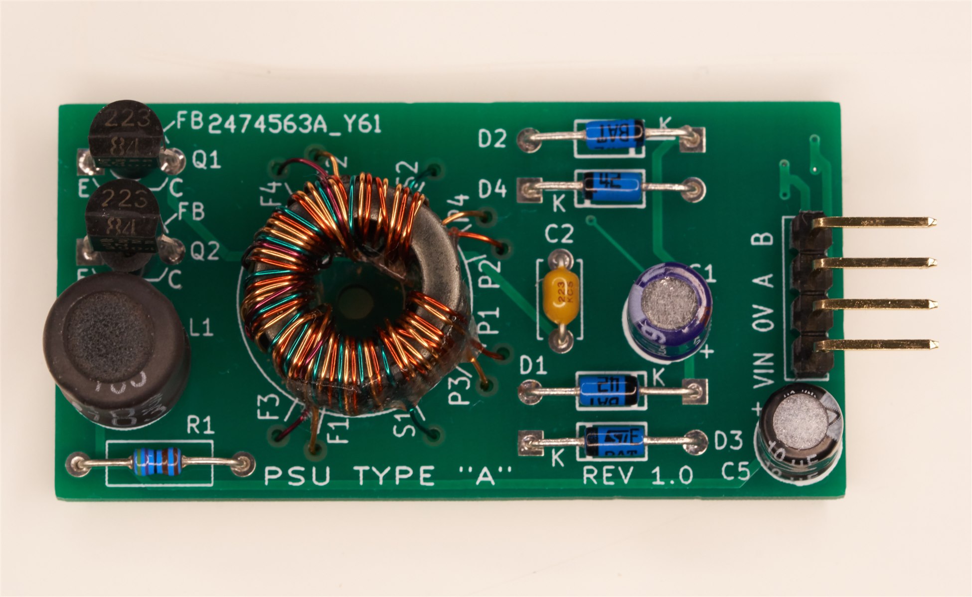
The project can be used with just three connections, arranged like a typical 78xx voltage regulator (the fourth connection visible on the board is only required when configured to be an isolated supply). The circuit board is larger than an LM7805 TO-220 part but not much larger than TO-220 on a typical heatsink. For my purposes, the size of the board didn’t matter; I was not seeking to miniaturize it.
For flexibility, the design described in this blog post can be configured for three different modes: either as a positive output supply, a negative output supply, or as a fully isolated output. There are shorting pads on the underside of the board to select any of these modes with a blob of solder. The shorting pads are labeled S1 to S6 in the board render below:
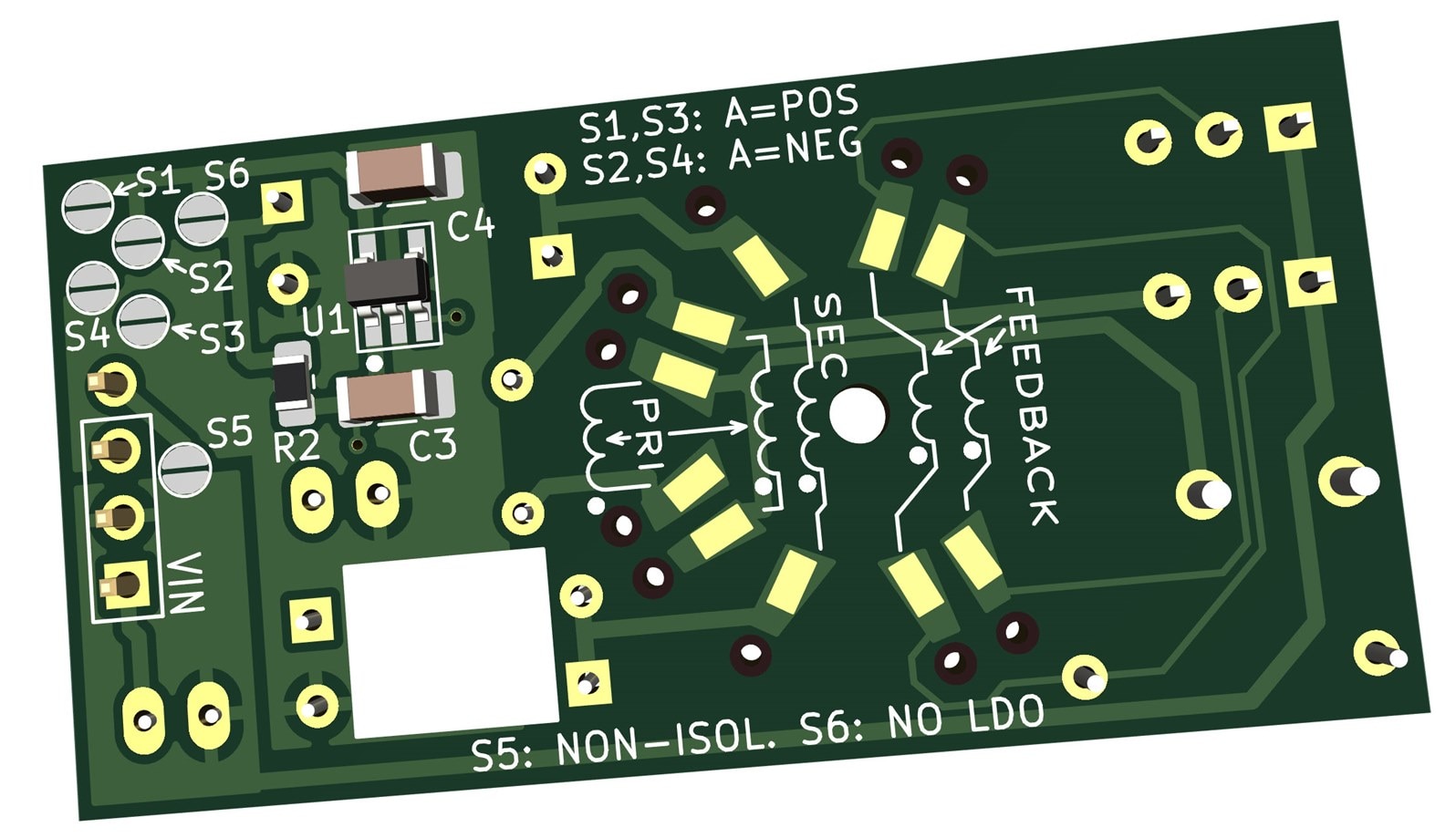
Furthermore, there is space on the underside to solder on an optional voltage regulator for even lower noise and stable output. The project is through-hole (since every component used has jellybean status, and it’s already fairly compact) unless you require the optional on-board voltage regulator, which is surface mount.
How Does it Work?
The design is based around a sine-wave oscillator, a bridge rectifier, and an optional linear voltage regulator.
Sine-Wave Oscillator
I needed an oscillator to convert the DC input voltage to AC so that it could be passed through a transformer to obtain an isolated output.
The chosen oscillator was designed originally by Peter Baxandall in the late 1950s, and he called it a current-switching oscillator. The key to it is the use of an inductor, which provides a constant current through the primary winding as the current is switched through the winding by the transistors. As a result of the constant current, instead of a square wave, this produces an approximate sine wave output if the frequency of oscillation and the load across the coil is just right. In practice, the output may not be a perfect sine wave and will change under load. Nevertheless, the fact that there is no sharp switching, plus the filtering and regulation, will all combine to hopefully produce a low-noise output.
Rectifier Circuit
The rectifier circuit is needed to convert the AC voltage into a (now isolated) DC voltage.
A simple bridge rectifier circuit was used, with Schottky diodes, to reduce the voltage drop slightly. A further improvement would be to use a center-tap winding from the Sine-Wave Oscillator stage to halve the voltage drop. For now, I have not made this improvement because it adds more complication to the transformer, and it’s already got enough of that.
Voltage Regulator
An optional voltage regulator is used to obtain a stable voltage and hopefully remove as much remaining ripple as possible. Some applications may not require a regulator. The choice of voltage regulator varies, depending on the requirement! For this project, the regulator has a maximum input of 5.5V, so some care is needed to ensure that the input doesn’t generate a voltage too high for it. If the voltage is high, then either fewer turns on the secondary of the transformer are needed, or an external regulator circuit should be used instead of the one on the PCB.
The selected voltage regulator was TLV740P, which comes in several fixed output variants. I used the 1.0V output version, called TLV74010.
Circuit
The entire circuit is shown below. Everything on the left forms the oscillator, where the two primary coils (with connections labeled P1-P2 and P3-P4) are responsible for the two halves of the sinewave cycle and are driven alternatively by the two transistors. C2 can be adjusted to determine the frequency of oscillation.
The dashed-box portion of the circuit is the optional voltage regulator. If this is not needed, then all the surface-mount components (R2, U1, C3, C4) can be omitted, and the pads labeled S6 (LDO_BYPASS) can be shorted with a blob of solder. The other pads labeled S1 to S5 can be optionally shorted to configure whether isolated output is required or non-isolated with the desired output polarity.
For example, if a regulated, non-isolated, negative output supply is needed, then S2, S4, and S5 must be shorted, and the negative output will appear on the third pin, which is labeled VA (the fourth pin, which is labeled VB, is only used in isolated output mode).

Building The Transformer
The steps to build the transformer are below.
| Ferrite Core | Ferrite Type | Wire Type | Wire Diameter |
| 5977001101 | 77 | Enameled | 0.2 - 0.32 mm |
Any enameled copper wire approximately 0.2 to 0.32 mm will be fine (thicker wire won’t fit, and thinner wire is too fiddly). If you’re going to be winding a lot of transformers, then it could be worthwhile buying different colors of wires, but there’s no issue with using just a single reel of wire and applying permanent markers to color the ends to identify each winding.
A total of five windings are needed, each one is referred to by the wire end connection names; for instance, P1-P2 is one primary winding. If the wires are cut to the sizes in the table, then there will be enough length for at least 5 cm of wire remaining at the start and the end of the windings.
| Winding | Description | Wire Length (cm) | Turns |
| P1-P2 | Primary | 57 | 20 |
| P3-P4 | Primary | 57 | 20 |
| S1-S2 | Secondary | 38 | 12 |
| F1-F2 | Feedback | 19 | 4 |
| F3-F4 | Feedback | 19 | 4 |
The photo here shows how the coil will be wound, but it is described in more detail below. In a nutshell, two wires (P1-P2 and P2-P3) are first wound (following the red arrow) until four turns have been wound. Then the wire labeled S1-S2 is wound as well (see the green arrow in the photo), so that now three wires are being simultaneously wound. Once S1-S2 is complete (12 windings according to the table above) then the P1-P2 and P3-P4 wires are wound for another four turns, so that they have a total of 4+12+4 windings, i.e., 20, which is in the table above.
Finally, two wires called F1-F2 and F3-F4 are wound for four turns. They are shown with the yellow arrow.
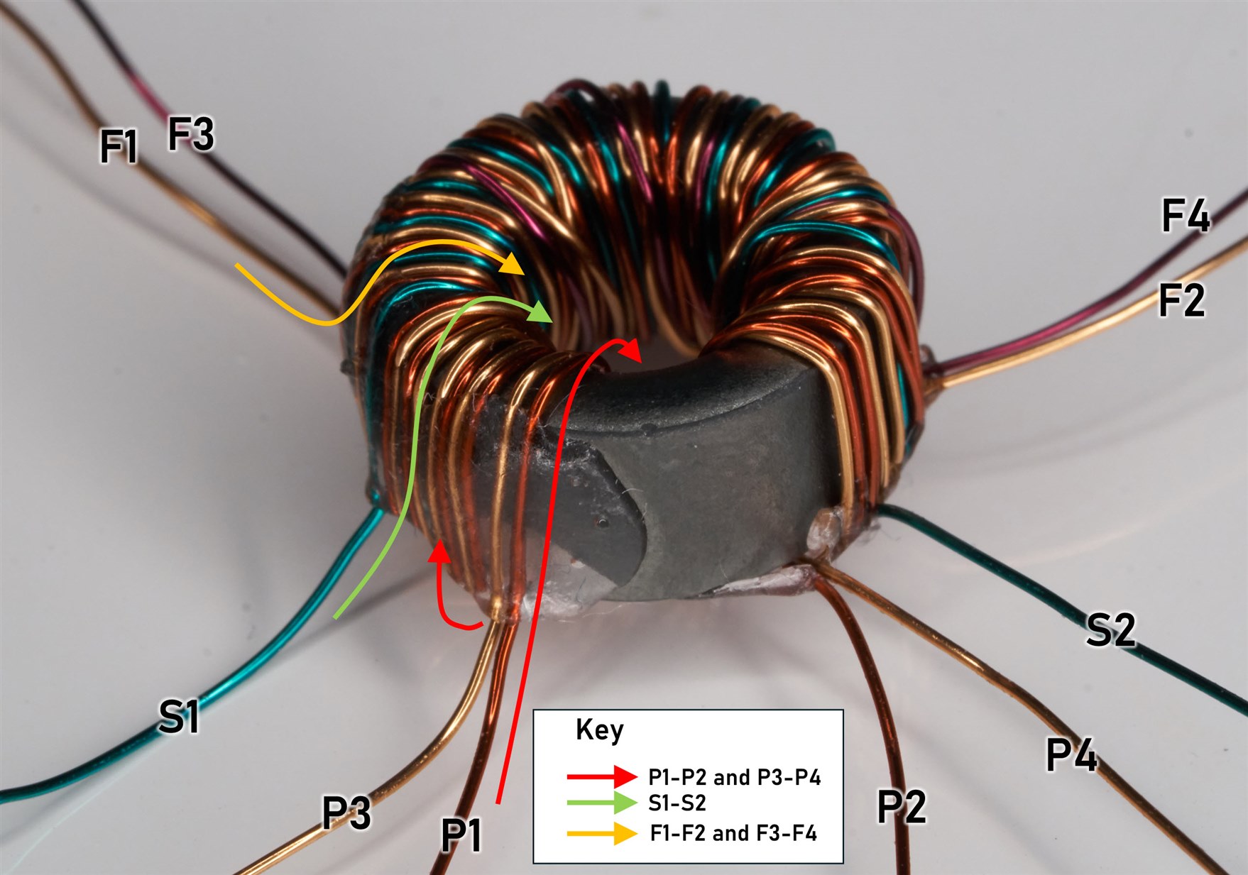
Wire Winding Procedure in More Detail
This isn’t difficult; it is a two-step procedure, and the photos can be used to see what is happening. I used 0.315 mm wire.
Step 1: Primary and Secondary Windings
Start with just the two Primary wires, hold them together in parallel, and wind them around the ferrite core for four turns. None of the windings need to be too neat, the wires can occasionally accidentally twist, so there’s no issue with that. Then add on the Secondary wire so that now you have three wires, and wind them all together for 12 more turns. Then wind just the two Primary wires for a further four turns. The end result will be three windings; the two Primary wires will have 20 turns (4+12+4), and the Secondary wire will have 12 turns. Secure the windings (e.g., with glue on the ends) and trim any excess wire so there is about 5 cm of wire free on each end.
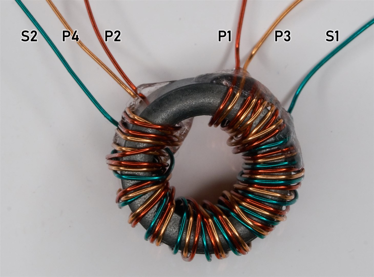
By now, the winding should look like the photo above. If the wire is only available in one color, then different-colored permanent markers can be applied at the wire ends before winding. In the photo above, the two Primary wires are red and gold, and the Secondary wire is green.
In the photo above, the winding was started with wire ends P1 and P3, and 4 turns were wound and then wire end S1 was added, and then the windings proceeded as discussed earlier.
Step 2: Feedback Windings
Next, at the other end of the ferrite core, take the two Feedback wires and wind them for four turns. Wind them in the same direction as all the other wires, just effectively rotated to the other side of the toroid. As before, secure the ends with glue and trim if there is excess wire remaining.
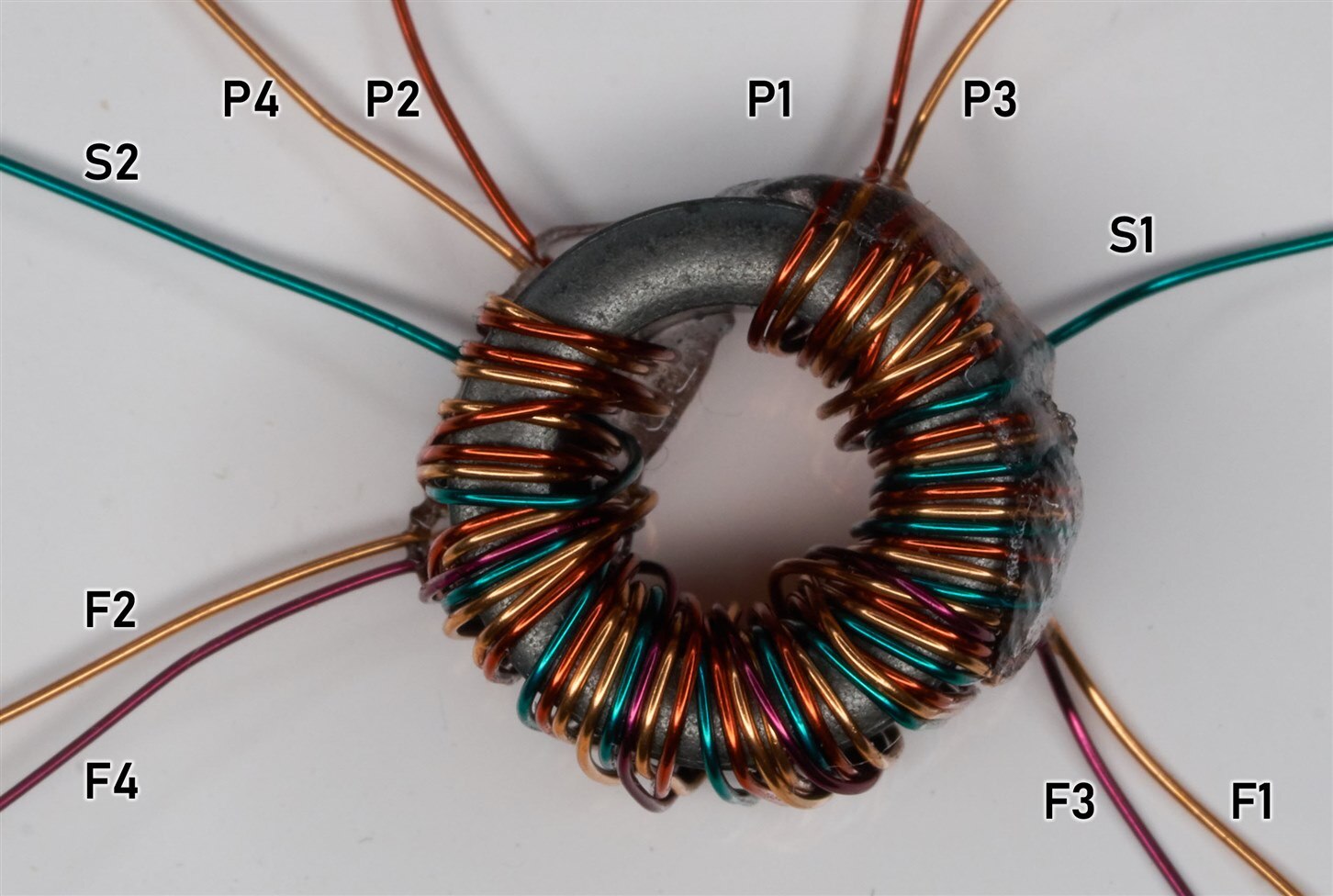
In the photo above, the feedback windings were started at ends F1 and F3, and were wound in the same direction as P1, P3, and S1. That’s it; the transformer windings are complete!
Transformer and Winding Tips
(a) Ferrite cores are very fragile; they will likely chip or break if they fall on a hard surface, so buying a spare one is a good idea.
(b) Each time the wires pass through the inside of the core, that is considered one turn. In the transformer photos above, the 12 turns of the green-colored secondary winding for instance, are easy to see; the winding was started on the right side (S1) with the wire first going over the top of the core and then down through the core.
(c) If you lose count, take a photo of the windings with a mobile phone camera, and then zoom in and count the turns.
(d) When winding pairs of wires, the ends can be twisted together, making threading them through the core easier.
(e) A suitable adhesive for the wire ends is “Solid Sticker Adhesive Gel,” which requires a UV flashlight to harden. It is putty-like and can be pressed into the wire ends and then illuminated for about 20 seconds (probably a good idea to keep your eyes shut during this time). Other options that I have not tried yet include hot glue, varnish, or nail polish.
(f) The enamel can be removed from the wire ends by putting a large blob of solder onto the soldering iron, positioning the wire inside the molten solder, and holding it there until the enamel smokes off.
Need a Different Voltage?
If a different output voltage is desired, then the number of turns on the secondary winding can be altered. However, the voltage drops under load, so some experimentation will be needed to achieve the optimal number.
If a regulated output is needed, then the output from the secondary winding must not exceed around 5Vp-p because the LDO input voltage range limit is 5.5V. If you’re unsure, then temporarily desolder R2 and measure the rectified output, to make sure it is no higher than 5V.
Assembling the Circuit
The transformer construction was nine-tenths of the assembly effort. Now, the remainder is easy. One thing not to forget (it is marked on the PCB silkscreen as a reminder) is the ferrite beads that the transistors are sitting on.. that helped reduce some RF emissions as was discovered in an earlier blog post.
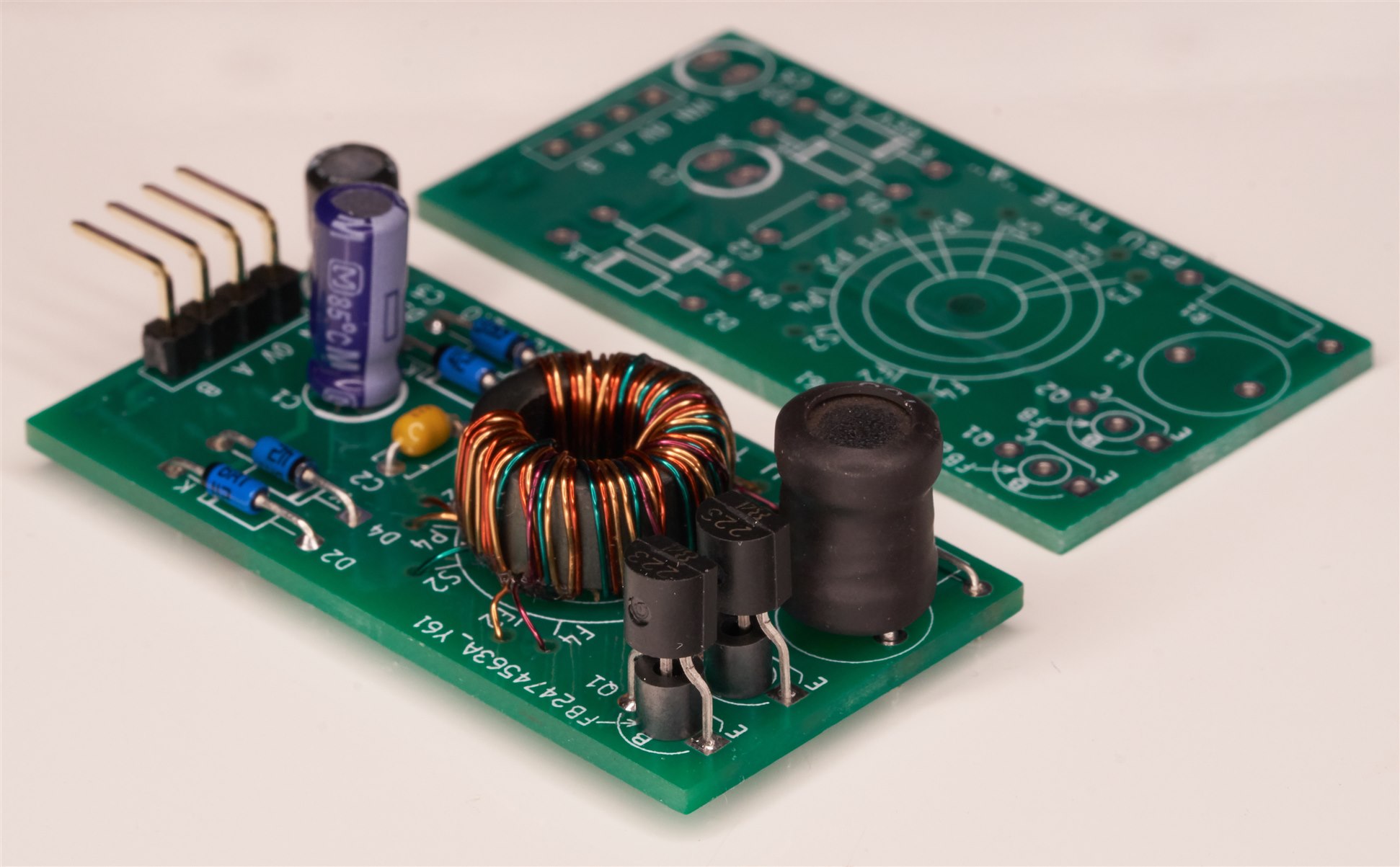
Initially, I didn’t solder the voltage regulator nor the bulk capacitor C1, so that I could obtain ‘scope traces of the partial circuit, and then I added C1 and measured the output to ensure it was below 5.5V because that’s the input voltage limit for the voltage regulator and I didn’t want to damage it.
The photo here shows the final assembled board underside, with the regulator and its associated components.
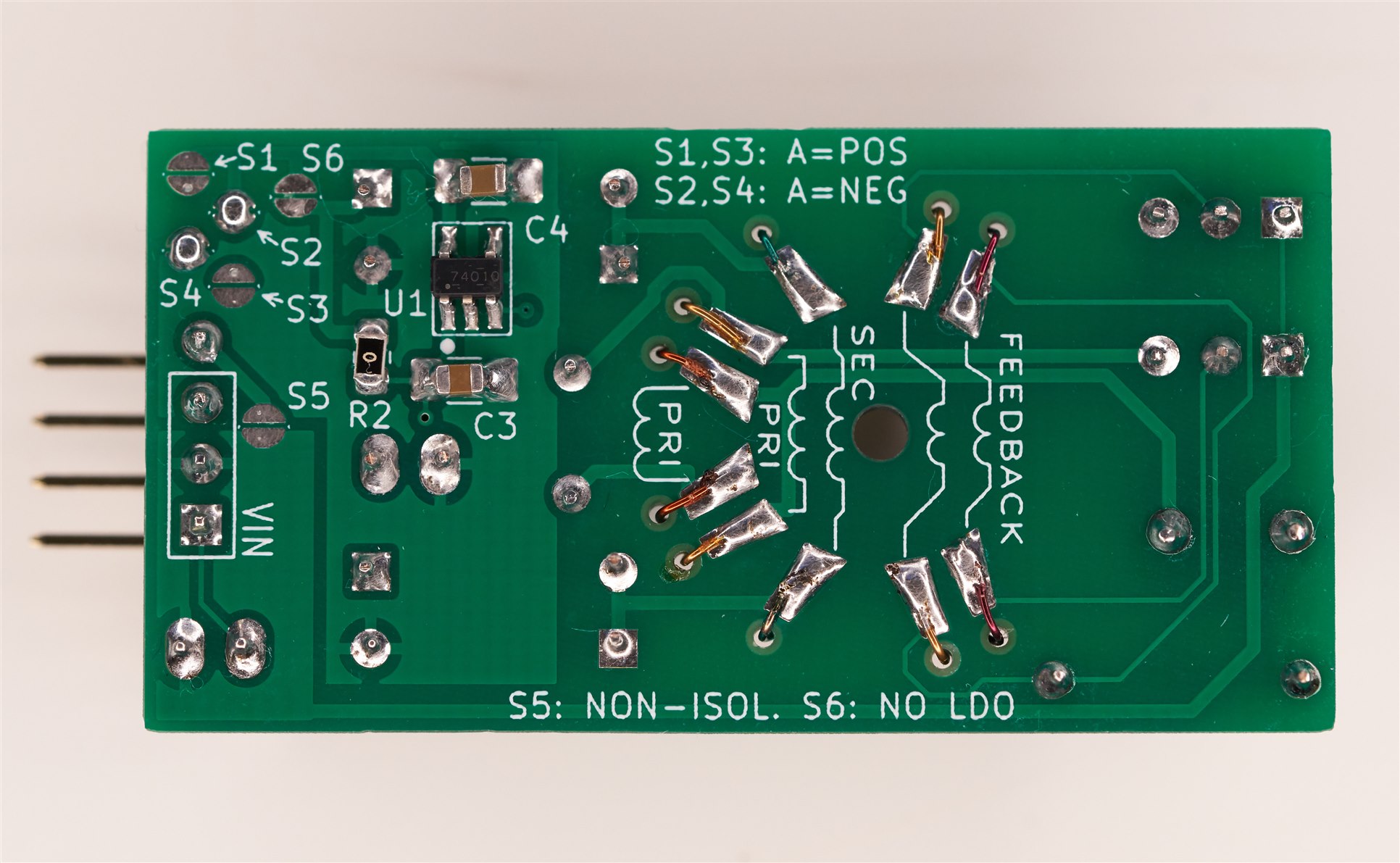
When soldering the transformer, all that needs to be done is to thread the transformer through the holes, crop the wires, and then heat the ends with a blob of molten solder to remove the enamel. Then, the wires are folded onto the board and soldered. The reason for the pads being this way is that I figured it could be easier for prototyping since the transformer can now easily be removed, rewound, and re-soldered.
The shorting links labeled S2 and S4 have been bridged with solder in the photo above, which means that the third pin outputs a negative voltage.
Traces
AC Output from the Transformer
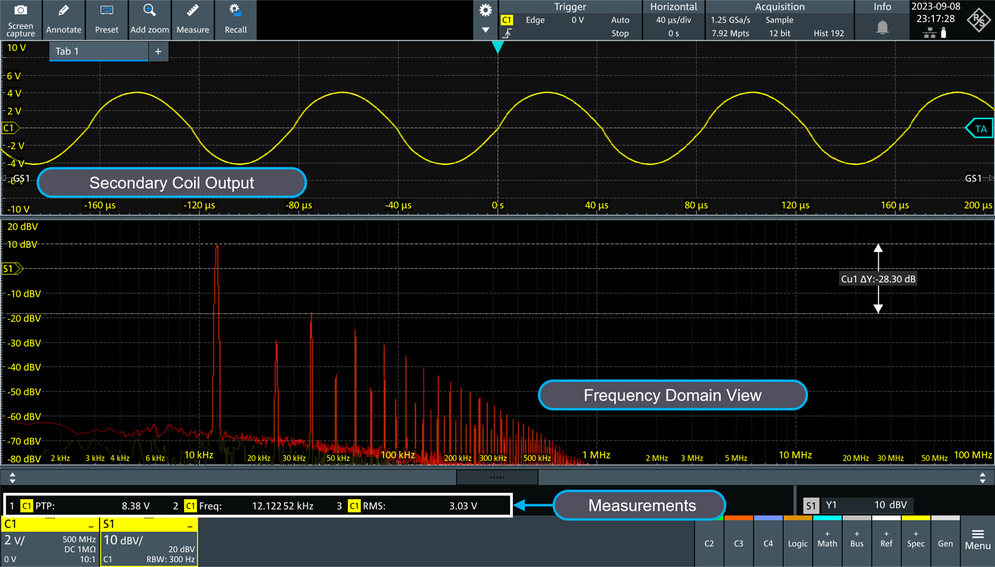
For an initial test, I powered the circuit from 5V and had no load on the output. The current consumption was about 20 mA. The ‘scope screenshot below shows the output probed on the secondary winding. As you can see, it’s an “almost” sinewave. There are harmonics, and it was possible to reduce their amplitude slightly with adjustments to the operating frequency of the circuit, but it can sometimes be better to have slightly higher amplitude harmonics, provided that the frequency is lower than smaller amplitude harmonics at a higher frequency. In any case, I was OK with the output for now because it will change slightly anyway when there is a load.
The spectrum view shows that the third harmonic is the highest, but it is still about 28 dB lower than the fundamental, which is pretty good!
Also, the frequency domain view shows that there’s not much output beyond 1 MHz, which is promising for subsequently adding a voltage regulator and removing a lot of noise.
Rectified Output at 5V Input
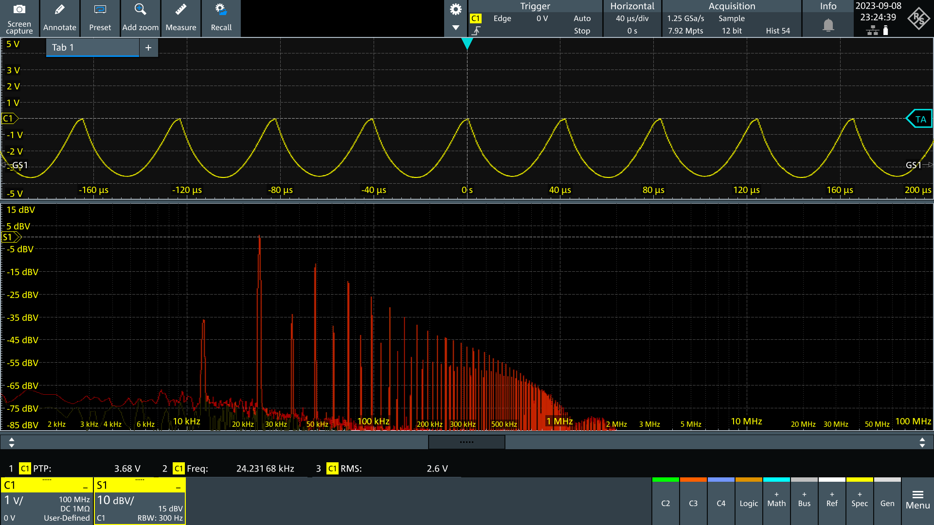
The screenshot below shows the rectified output without any output capacitor attached. Again, the input voltage was 5V to the circuit. The rectification looks “upside-down” simply because I wanted to create a negative rail, and I connected the ‘scope probe accordingly. The rectified output was 2.6 Vrms (see the measurements displayed just below the spectrum view on the screenshot). The spectrum view reveals some output beyond 1 MHz, which I assumed was not good because that would be more difficult to remove from the final output from the circuit.
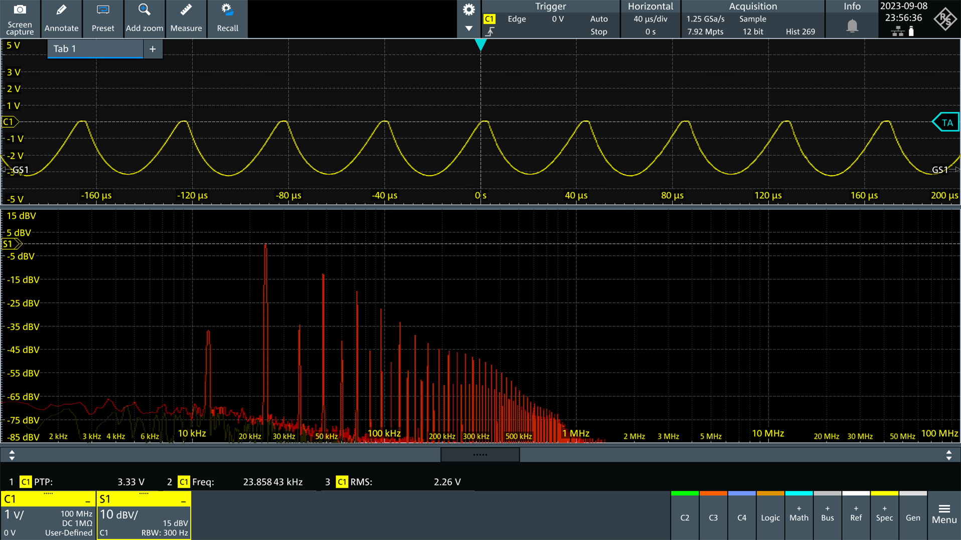
The next screenshot shows the rectified output when there is a 220-ohm load present. The measurement at the bottom of the screenshot shows that the output is now 2.26 Vrms.
Rectified Output at 3V Input
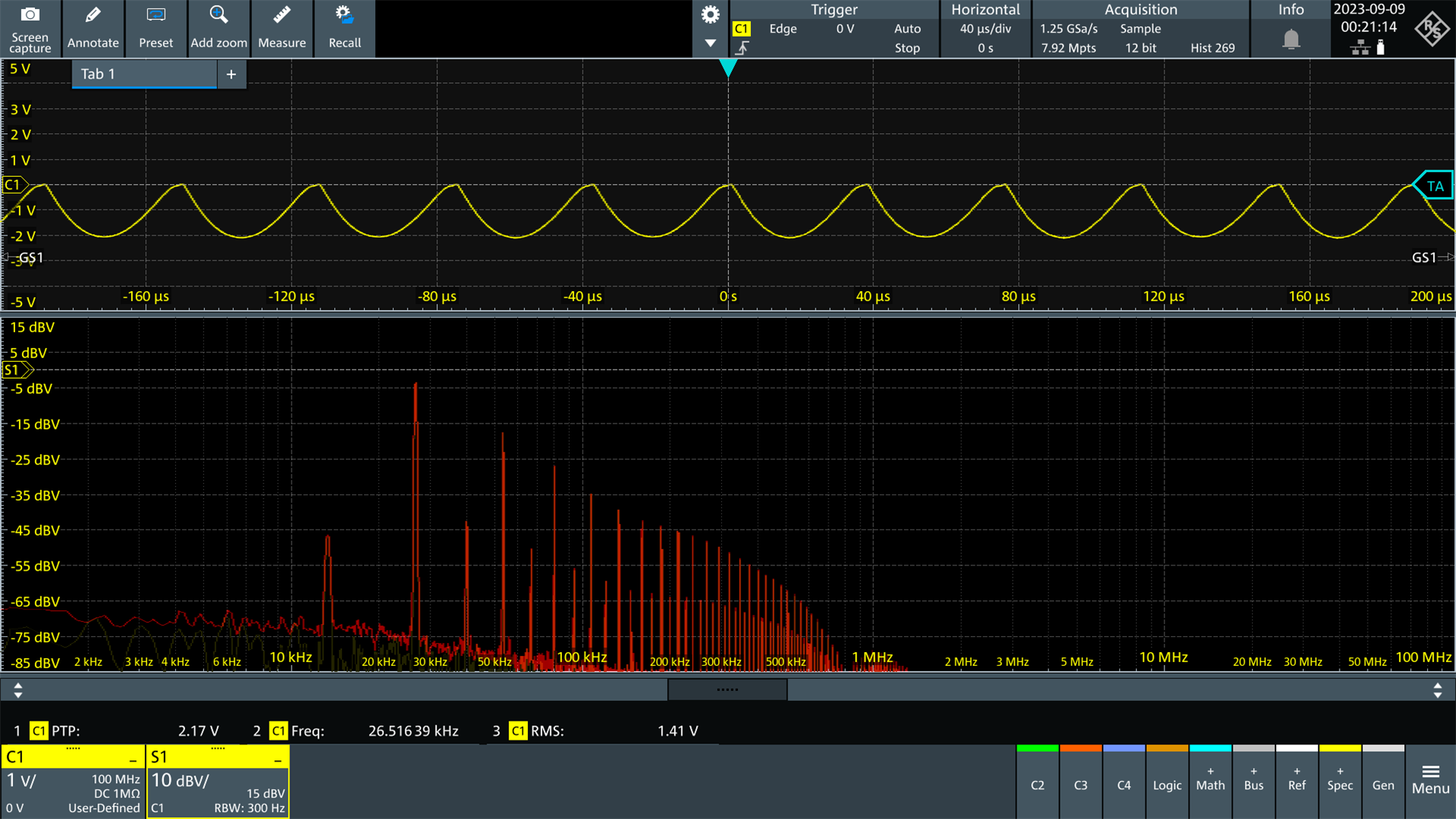
Here’s the scope view when the source voltage is set to 3V. There is no load present. The output is 1.41V RMS.
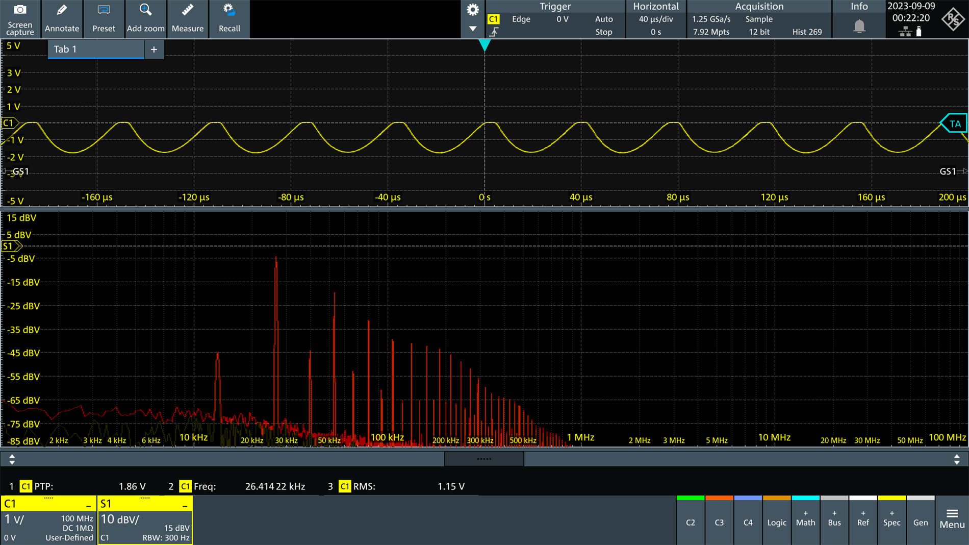
The screenshot below shows what happens when a 220-ohm load is applied. The output reduces to 1.15V RMS.
Output After Bulk Capacitor Ripple Reduction
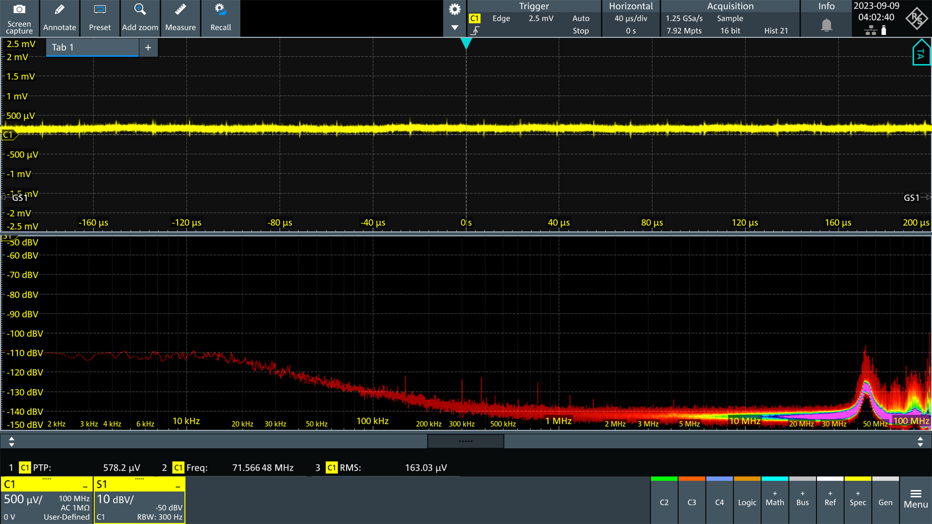
Once capacitor C1 was added to the circuit (but no voltage regulator), the output was observed, this time with the ‘scope set to AC coupling. This was with no power applied, so I could see what noise was present without running the test:
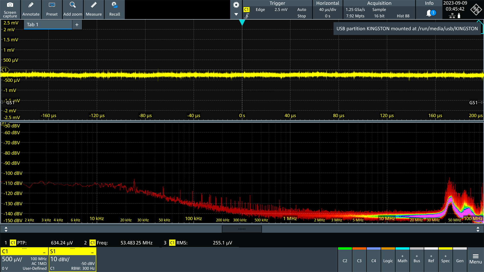
Next, with 5V power applied. the screenshot below shows the result with no load. Not much difference!
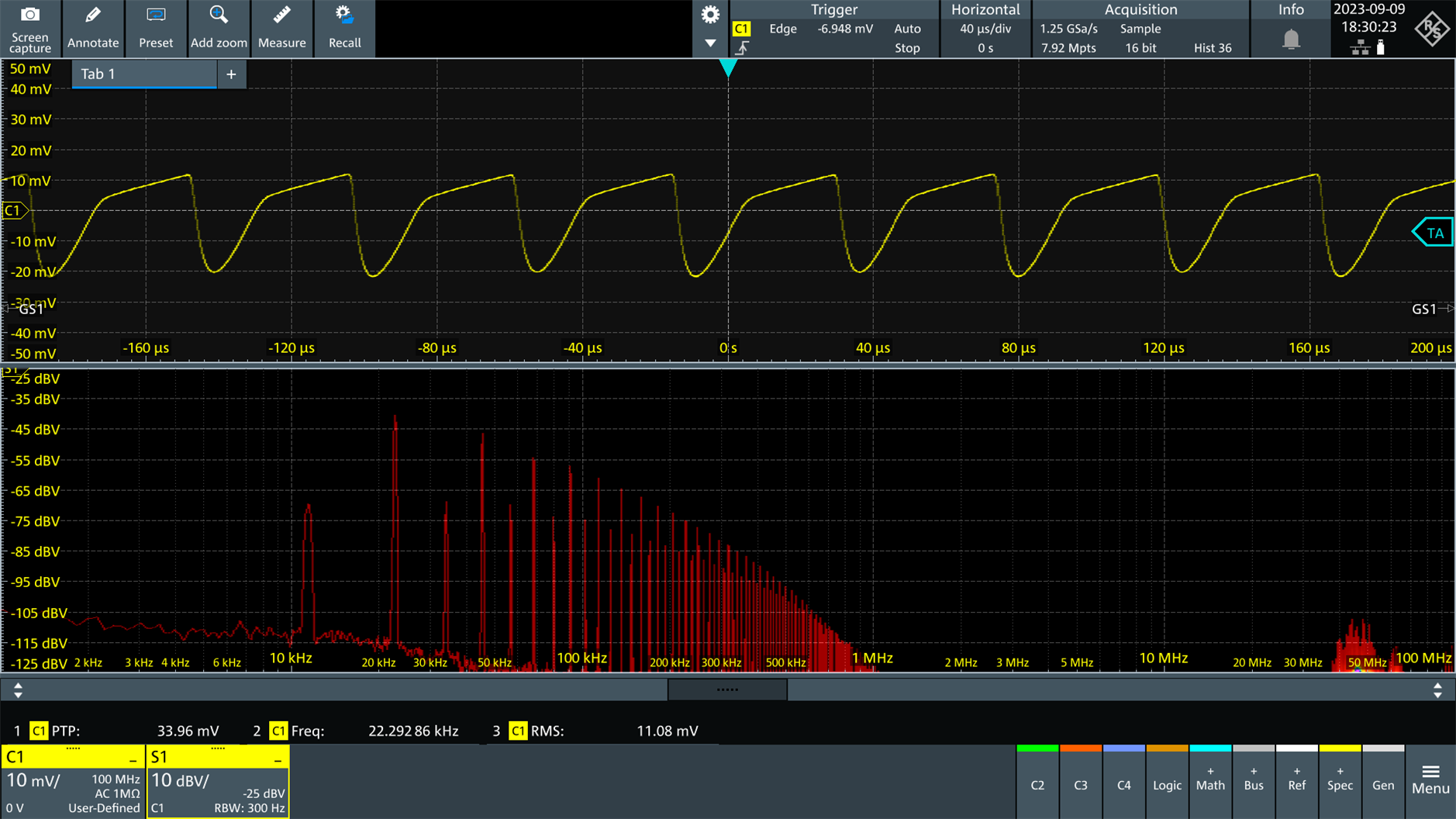
With a 220-ohm load, the result is shown below. All the noise (which of course is primarily harmonics) tails off beyond 1 MHz (the bit of red at around 50 MHz is not related since it was present even when powered off).
Regulated Output with 5V Input
With a TLV7401 regulator soldered on, a -1V rail was expected. Here is what the output looked like (‘scope set to AC coupling), with a 220-ohm load:
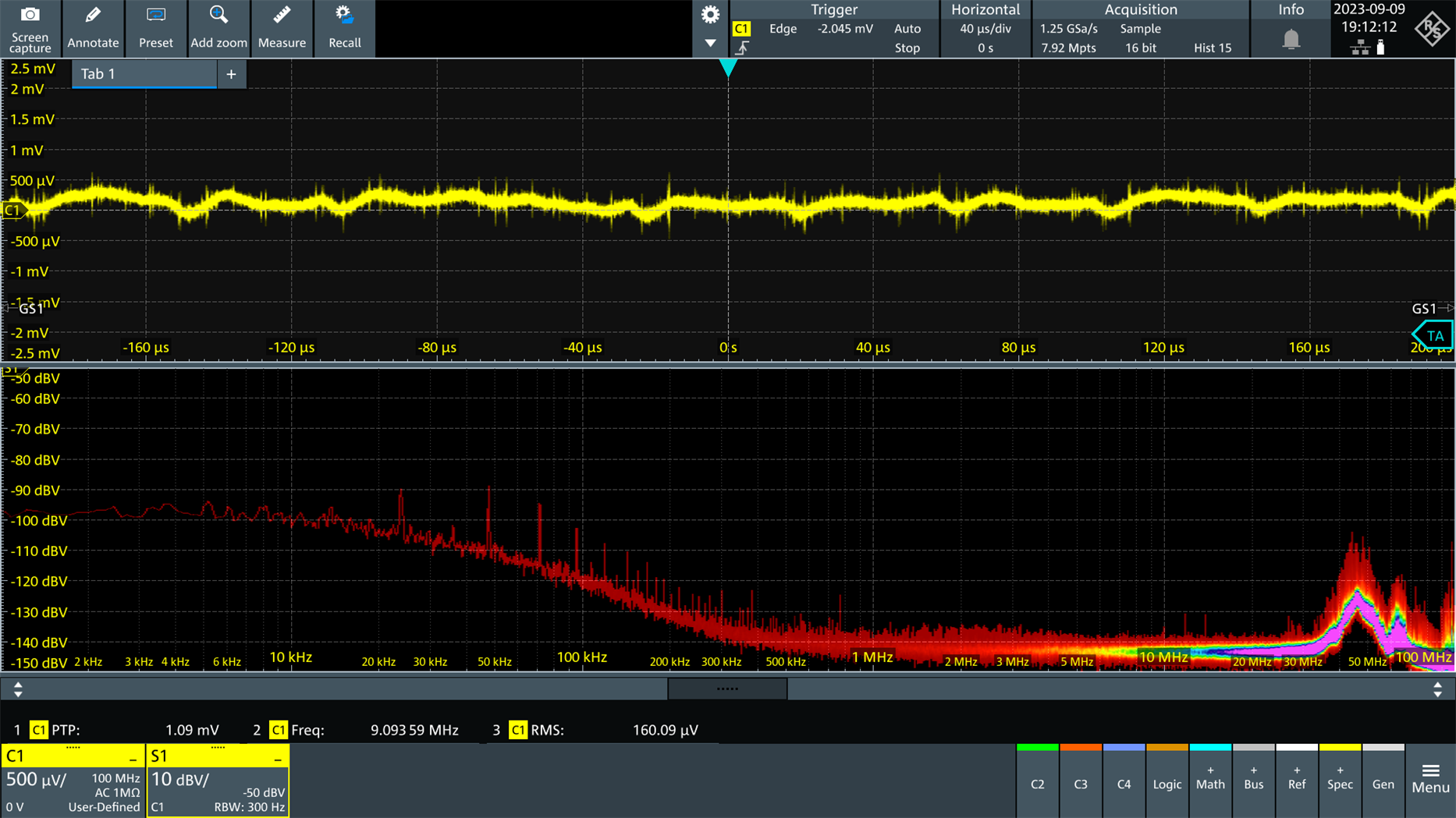
According to the measurement at the bottom of the ‘scope display shown above, that’s 160 uV RMS, with a 100 MHz bandwidth, but the actual noise will be lower since there is some noise from the testbed that I couldn’t get rid of.
That’s pretty reasonable, considering that just about the cheapest parts have been used! Replacing the voltage regulator with the more expensive TPS7A20 would make quite a difference, perhaps. However, with the circuit as-is, I’d be happy to use it for a negative rail for an op-amp.
Current Consumption
Now that the circuit was complete, I took some measurements. The output voltage is -1V, since that is what the chosen voltage regulator outputs.
I simply powered the circuit from 3.1V to 5V and measured the current consumption with different loads applied.
| Input Voltage | Quiescent Current (No load) | Current Consumption with 4.5 mA load (220 ohm) | Current Consumption with 10 mA load (100 ohm) |
| 3.1 V | 8.8 mA | 12.7 mA | Out of Regulation |
| 3.3 V | 9.6 mA | 13.6 mA | Out of Regulation |
| 3.4 V | 10.1 mA | 14.0 mA | 18.5 mA |
| 5.0 V | 17.6 mA | 21.4 mA | 25.8 mA |
5V Input:
| Load | Current Consumption |
| 10 mA | 25.8 mA |
| 20 mA | 33.5 mA |
| 30 mA | 40.9 mA |
| 40 mA | 48.4 mA |
Beyond about 45 mA, the output collapses.
Summary
This was an interesting project, trying to improve the noise performance compared to existing DC-DC converters. The final result is a fairly flexible power supply board that can be configured for positive or negative rails and isolated if desired. The project is extremely low-cost (about $3), provided some enamel wire is available. The circuit board is suitable for any low-voltage and low-current requirement, with optional onboard voltage regulation up to 3.3V depending on the particular regulator IC soldered on.
A future board may be designed for higher voltage and higher current outputs, and with perhaps dual isolated rails (that would be a separate blog post if it happens).
Although the output is low noise, trying a higher-end voltage regulator could be an interesting modification. Another thing worth trying would be to separate the primary and secondary windings so that they are not overlapping; then, there would be less noise capacitively coupled from the primary side to the secondary, and vice-versa. However, that may require a slightly larger ferrite core since there was not much space on the current core used.
Thanks for reading!


Top Comments
-

Jan Cumps
-
Cancel
-
Vote Up
0
Vote Down
-
-
Sign in to reply
-
More
-
Cancel
Comment-

Jan Cumps
-
Cancel
-
Vote Up
0
Vote Down
-
-
Sign in to reply
-
More
-
Cancel
Children