Table of Contents
Introduction
I’ve got through a lot of model “1798” power supplies! They come with Surface laptops, and they don’t seem to last much beyond a couple of years.

(image source: Microsoft website)
Just out of curiosity, here is a teardown of one, so we can see how it operates. Note: it’s not possible to repair these, it is a destructive teardown because the plastic case is welded shut, and there are metal shields and an insulating cement which needs to be chipped away in places.
I was wondering why these power bricks cost £100. After tearing it down, now I realize why, and I don’t feel so bad having to buy another one. But first, for a comparison, here’s what a cheap clone can look like on the inside, courtesy of Big Clive:

(Image source: Big Clive video)
It’s worth watching the Big Clive video, to see how such a charger can destroy a laptop and external monitor!
Removing the Case and Shielding
The case needs to be milled off. It’s not going to come apart anytime soon even with a hacksaw, without a lot of damage. Milling reduces the chances of wrecking it further. Inside, the power supply has a copper shield surrounding it. I liked that the mains connector, and the USB connector, are “floating” so that they do not cause stress on the PCB when plugged/unplugged.
Notice that the main charging lead has four connections, not just two! The two thin wires detect when the magnetic connector is fully attached, and then turn on the supply. The cheap clone chargers omit this, and (presumably) cause arcing and damage to the laptop.

The magnetic connector:

Another photo showing lots of copper shielding.

I snipped off the shielding connections, and then bent off the heatshinks although I could have unsoldered them the PCB. Parts are attached to the heatsinks using thermally conductive adhesive tape, and they came off fine.

What Parts are Used?
There’s a lot of wound components, so that’s going to be a significant part of the expense. The entire supply is custom (manufactured by Chicony).
Most of the MOSFETs are from Infineon, and the power factor correction (PFC) and power supply controller IC are from NXP.
The bridge rectifier is a Diodes Inc GBP808N, capable of 8A with a heatsink (the parts on the side of the board were connected to a heatsink plate, which I've removed and is not shown). Power factor correction uses the NXP TEA19162T, along with a ST STTH5L06 600V 5A ultrafast rectifier, and IPD60R380P6 Infineon CoolMOS P6 N-channel MOSFET.

A view of the mains filter portion:

Power factor correction (PFC) chip TEA19162T was buried under the white stuff:

The STTH5L06 rectifier:

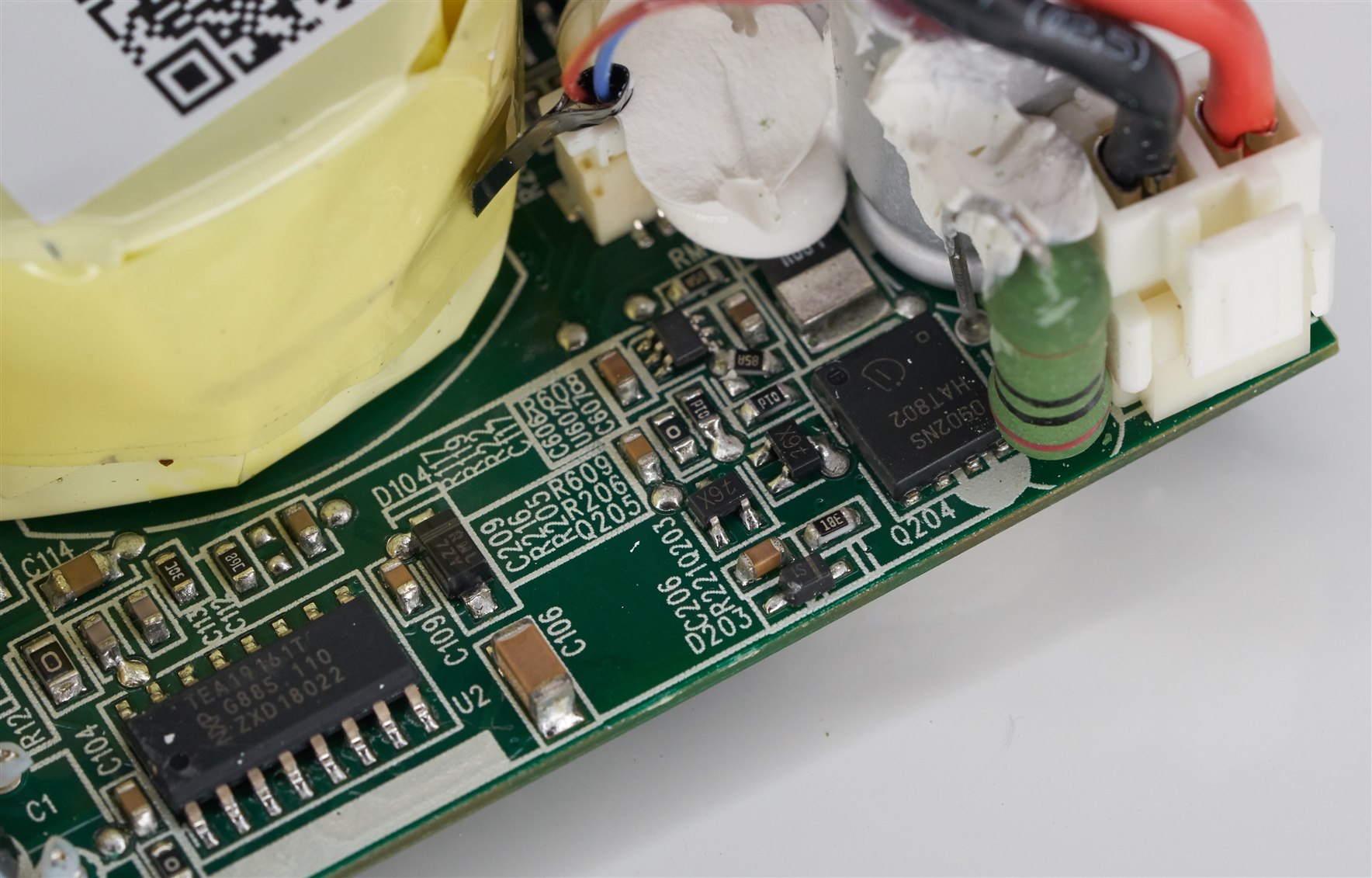
An NXP TEA19161T (the 16-pin SOIC in the photo below) is used as the switching controller for a resonant supply.

Close-up view of that area:

The transformer looks custom, and is pretty compact (about 30x30x18mm) considering it needs to support just over 100W.
Here's the STFH24N60M2 N-ch 600V MOSFET used for the resonant converter:

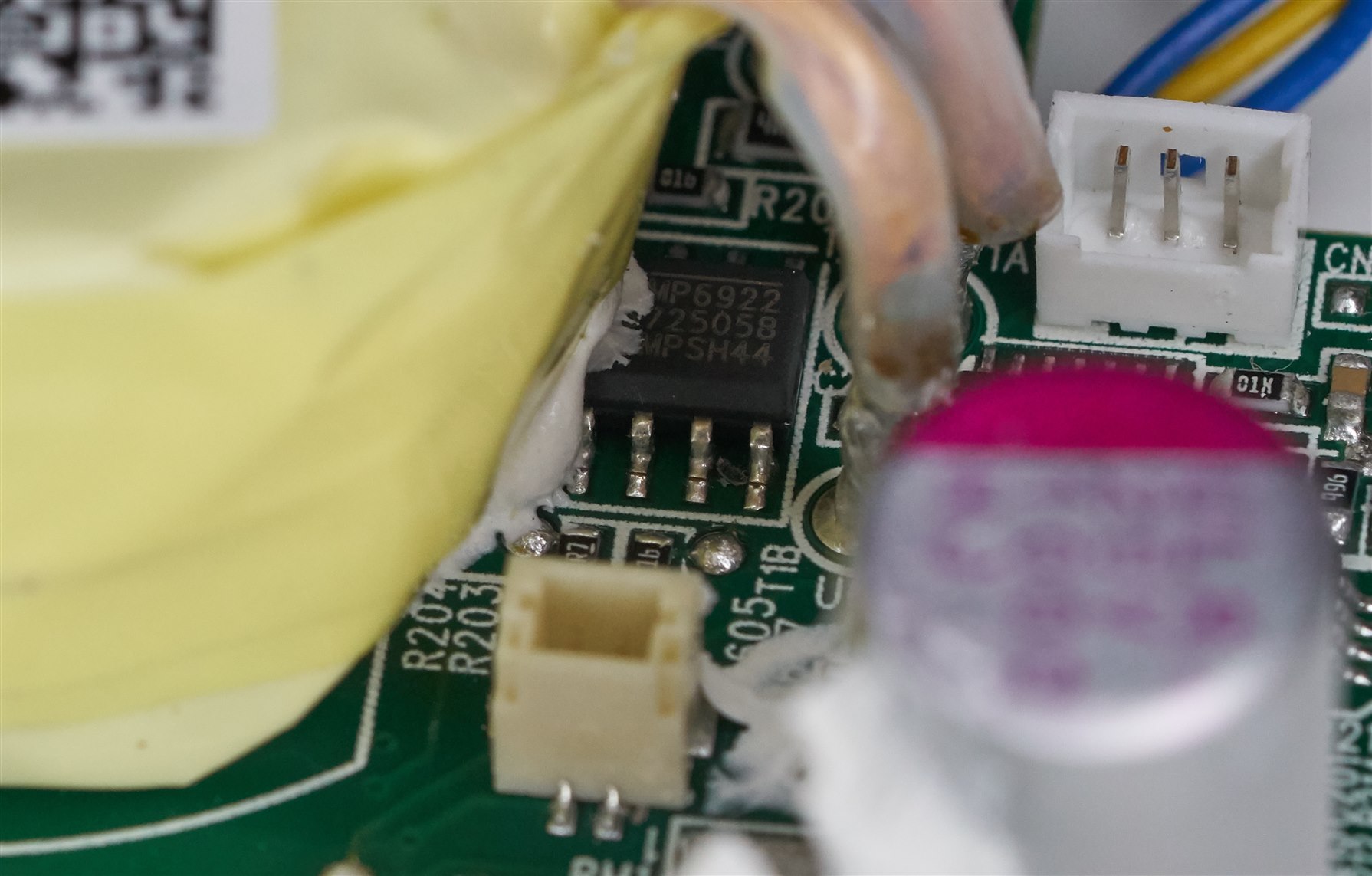
On the DC output side, a MPS MP6922 MOSFET controller (the 8-pin SOIC in the photo below) is used, to control a couple of AOL1240 N-channel MOSFETs, to perform synchronous rectification (i.e. used as active diodes) for higher efficiency.

MOSFETs excavated from the white stuff on the other side:

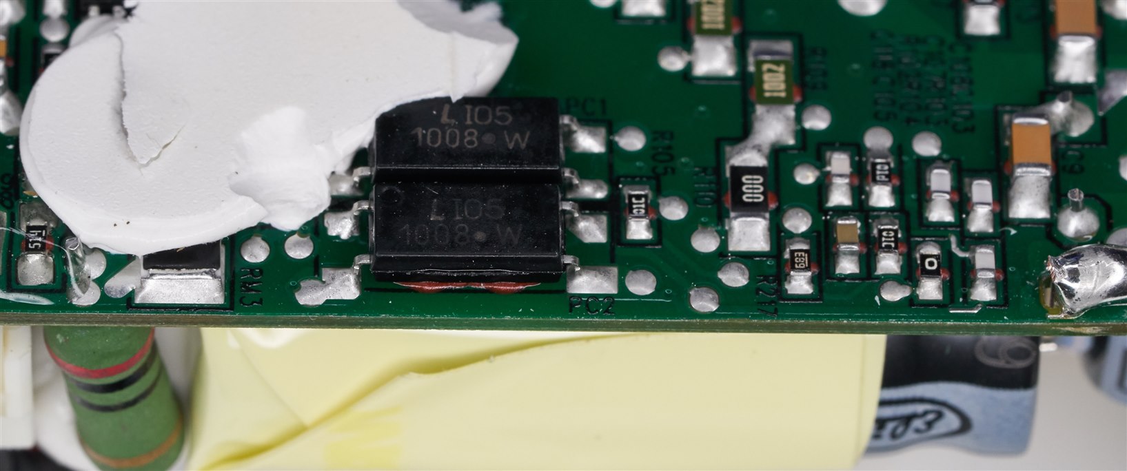
Opto-isolators:

There is a SSOP-14 part labelled SH3H0003S that I couldn’t find any information for, but I believe it is related to the USB power output connector (the power brick has a separate USB output intended for charging phones and so on).

Underside of the USB board:

There’s also an INA213 chip and a sense resistor, so current is actually monitored, and there’s a MOSFET to switch the supply on or off, presumably under control of the two thin wires within the DC output cable.
All-in-all, I can see that the power supply probably is worth the £100. It’s just a pity it doesn’t last all that long. However, on the plus side, there’s a newer compatible model 1932, and that may last longer.
Thanks for reading!

.jpg)