element14 Community
element14 Community
    Register Log In
  • Site
  • Search
  • Log In Register
  • About Us
  • Community Hub
    Community Hub
    • What's New on element14
    • Feedback and Support
    • Benefits of Membership
    • Personal Blogs
    • Members Area
    • Achievement Levels
  • Learn
    Learn
    • Ask an Expert
    • eBooks
    • element14 presents
    • Learning Center
    • Tech Spotlight
    • STEM Academy
    • Webinars, Training and Events
    • Learning Groups
  • Technologies
    Technologies
    • 3D Printing
    • FPGA
    • Industrial Automation
    • Internet of Things
    • Power & Energy
    • Sensors
    • Technology Groups
  • Challenges & Projects
    Challenges & Projects
    • Design Challenges
    • element14 presents Projects
    • Project14
    • Arduino Projects
    • Raspberry Pi Projects
    • Project Groups
  • Products
    Products
    • Arduino
    • Avnet Boards Community
    • Dev Tools
    • Manufacturers
    • Multicomp Pro
    • Product Groups
    • Raspberry Pi
    • RoadTests & Reviews
  • Store
    Store
    • Visit Your Store
    • Choose another store...
      • Europe
      •  Austria (German)
      •  Belgium (Dutch, French)
      •  Bulgaria (Bulgarian)
      •  Czech Republic (Czech)
      •  Denmark (Danish)
      •  Estonia (Estonian)
      •  Finland (Finnish)
      •  France (French)
      •  Germany (German)
      •  Hungary (Hungarian)
      •  Ireland
      •  Israel
      •  Italy (Italian)
      •  Latvia (Latvian)
      •  
      •  Lithuania (Lithuanian)
      •  Netherlands (Dutch)
      •  Norway (Norwegian)
      •  Poland (Polish)
      •  Portugal (Portuguese)
      •  Romania (Romanian)
      •  Russia (Russian)
      •  Slovakia (Slovak)
      •  Slovenia (Slovenian)
      •  Spain (Spanish)
      •  Sweden (Swedish)
      •  Switzerland(German, French)
      •  Turkey (Turkish)
      •  United Kingdom
      • Asia Pacific
      •  Australia
      •  China
      •  Hong Kong
      •  India
      •  Korea (Korean)
      •  Malaysia
      •  New Zealand
      •  Philippines
      •  Singapore
      •  Taiwan
      •  Thailand (Thai)
      • Americas
      •  Brazil (Portuguese)
      •  Canada
      •  Mexico (Spanish)
      •  United States
      Can't find the country/region you're looking for? Visit our export site or find a local distributor.
  • Translate
  • Profile
  • Settings
Power & Energy
  • Technologies
  • More
Power & Energy
Forum Issues With MOSFET bridge, DC motor 24V 200W
  • Blog
  • Forum
  • Quiz
  • Documents
  • Polls
  • Events
  • Mentions
  • Sub-Groups
  • Tags
  • More
  • Cancel
  • New
Actions
  • Share
  • More
  • Cancel
Forum Thread Details
  • State Suggested Answer
  • Replies 10 replies
  • Answers 2 answers
  • Subscribers 286 subscribers
  • Views 4289 views
  • Users 0 members are here
  • mosfet
  • motor drives
  • mosfet driver
  • h bridge circuit
  • brushed dc motor control
  • h bridge motor control
  • high side driver
Related

Issues With MOSFET bridge, DC motor 24V 200W

shwetankv007
shwetankv007 over 4 years ago

Hello everyone,

I have been working on a project to drive a 200W 24V motor that gets a continuous drive current of about 7-8A. The idea is to run the motor in forward and reverse direction interchangeably much like a car viper. The time for forward and reverse is about 20seconds each.

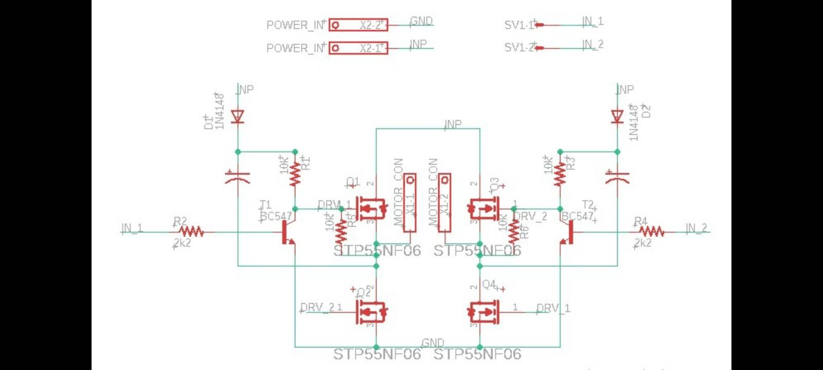
I want to use 4-N channel MOSFETs for this and use a discrete driver.

Mosfets used - STP55N i.e. 60V 50A

Input supply - 24V

PWM input - In-1 and In-2, a signal on one of the inputs will run the motor in one direction and vice versa.

Bootstrap Capacitor - 10uF 50V


Issues -

1. The circuit is working i.e. motor is getting turned on in both the direction but upper MOSFETs are getting heated upto 70degree within few minutes.

2. Is there an issue with the bootstrap circuitry?

image

  • Sign in to reply
  • Cancel

Top Replies

  • kkazem
    kkazem over 3 years ago +3
    It's a bad idea to drive a power mosfet this way. First of all, the Supply Voltage is 24 VDC and the FET's max gate voltage is only 20 V. Therefore, you can expect FET failures via puncturing the gate…
  • dougw
    dougw over 4 years ago +2 suggested
    R1 may be too high of a value. It will take time to charge the gate capacitance, which will turn the FET on slowly, causing heat losses. If R1 is made smaller, it may discharge the capacitor too fast to…
  • dougw
    dougw over 4 years ago in reply to shwetankv007 +1
    Is the capacitor discharging when T1 is on to the point where there is no boost to the gate - which would mean Q1 is only partly turned on? By push-pull I mean put a stage like this on the output of T1…
  • dougw
    0 dougw over 4 years ago

    R1 may be too high of a value. It will take time to charge the gate capacitance, which will turn the FET on slowly, causing heat losses.

    If R1 is made smaller, it may discharge the capacitor too fast to keep the FET on.

    You may need to drive the gate with a push pull transistor pair so it turns on and off quickly without discharging the capacitor.

    You also need to ensure that Q1 and Q2 are never turned on at the same time. If Q1 is slow to turn off, Q2 will pull current through it, heating it up.

    The same problem happens to Q2 if it is slow to turn off.

    You need a delay between turning each FET off and turning its counterpart on.

    • Cancel
    • Vote Up +2 Vote Down
    • Sign in to reply
    • Verify Answer
    • Reject Answer
    • Cancel
  • shwetankv007
    0 shwetankv007 over 4 years ago in reply to dougw

    When you say to drive the gate with a push pull pair, are you referring to both High side and Low side FETs.

    For experiment, I gave IN_1 a permanent zero volt and IN_2 a permanent 5V. Turning on Q1 and Q4. Do I still need to consider the rise time since the gate is always ON?


    Also, the Ciss is around 1.5nF that will give me a rise time of 15us roughly with the 10K resistor. If I use a PWM of 10KHz, then also this rise time may work ?

    • Cancel
    • Vote Up 0 Vote Down
    • Sign in to reply
    • Verify Answer
    • Cancel
  • dougw
    0 dougw over 4 years ago in reply to shwetankv007

    Is the capacitor discharging when T1 is on to the point where there is no boost to the gate - which would mean Q1 is only partly turned on?

    By push-pull I mean put a stage like this on the output of T1, this would allow a large value for R1 that would not discharge the capacitor so fast:

    image

    • Cancel
    • Vote Up +1 Vote Down
    • Sign in to reply
    • Verify Answer
    • Cancel
  • robogary
    0 robogary over 4 years ago

    Maybe take a look with a scope to see if you are getting shoot thru, i.e. forward and reverse bridges firing at the same time or with some overlap.

    Do bridges have solid interlocking and deadband ?

    Are you running no load, or with load ?  Try running motor uncoupled to see if heating changes significantly.

    • Cancel
    • Vote Up +1 Vote Down
    • Sign in to reply
    • Verify Answer
    • Reject Answer
    • Cancel
  • shwetankv007
    0 shwetankv007 over 4 years ago in reply to dougw

    Got that, this will help me reduce the charging slope during the positive and negative triggers. Tried this circuit too for feeding to the gate, still the upper MOSFET is heating.


    Some more observations :-

    At Supply voltage 27V, when T1 base is pulled down and T2 pulled up.

    Gate voltage at Q1 is 25V, Drain source voltage at Q1 is 2.5 volts and Drain source voltage at Q4 is zero.

    This suggests that Q1 is not turning on properly.


    Is the bootstrap not working correctly? Am I missing something?

    Thanks

    • Cancel
    • Vote Up 0 Vote Down
    • Sign in to reply
    • Verify Answer
    • Cancel
  • shwetankv007
    0 shwetankv007 over 4 years ago in reply to robogary

    On no load it is working fine. As I apply some load to it, the upper MOSFET starts heating. And I checked there are no shoot thru, apparently the other two MOSFETs stay off during the whole process.

    As far as the deadband is concerned, I am giving 100% duty to the Q1 and Q3 MOSFET and zero duty to other to.

    I got some measurements though,


    At Supply voltage 27V, when T1 base is pulled down and T2 pulled up.

    Gate voltage at Q1 is 25V, Drain source voltage at Q1 is 2.5 volts and Drain source voltage at Q4 is zero.


    Does this suggests anything?

    Thanks

    • Cancel
    • Vote Up 0 Vote Down
    • Sign in to reply
    • Verify Answer
    • Cancel
  • dougw
    0 dougw over 4 years ago in reply to shwetankv007

    It sounds like you should remove the pull down resistor on the gate of Q1.

    Or maybe it should be between the Q1 gate and T1 collector.

    • Cancel
    • Vote Up +1 Vote Down
    • Sign in to reply
    • Verify Answer
    • Cancel
  • shwetankv007
    0 shwetankv007 over 4 years ago in reply to dougw

    Yes I tried to remove the pull down  resistor - same effect.

    Will try with multiple iterations of series gate resistance and see if I get any better response.

    Thanks

    • Cancel
    • Vote Up 0 Vote Down
    • Sign in to reply
    • Verify Answer
    • Cancel
  • dougw
    0 dougw over 4 years ago in reply to shwetankv007

    What is the voltage on the boost capacitor? It seems it is not high enough...

    • Cancel
    • Vote Up 0 Vote Down
    • Sign in to reply
    • Verify Answer
    • Cancel
  • kkazem
    0 kkazem over 3 years ago

    It's a bad idea to drive a power mosfet this way. First of all, the Supply Voltage is 24 VDC and the FET's max gate voltage is only 20 V. Therefore, you can expect FET failures via puncturing the gate, though it probably won't happen right away.  Second, as the turn on path is thru a 10K resistor, the maximum gate charge current is only 2.4 mA peak and reduces as the gate charges up. This would translate into a turn on time of about 37 uS, which is much slower than optimal, causing high FET switching losses. It's not as bad for turn off as the T1 NPN can sink 100-300 mA. A proper FET driver should source and sink at least 1.5 amps for a FET this size for fast switching in the 50-200 nSec range. A cascade (totem-pole) NPN-PNP arrangement (or n-CH-p-CH in MOS) using discrete parts can be used, but the drive supply should be limited to 12 to 15 VDC typically. Even if the FET gate is rated at +/-30V, there's no real advantage to driving the gates that high as they're typically fully enhanced at 10-12 V Vgs. One good, low-cost method for gate drive is to use a CMOS hex inverter or buffer and parallel all of them. Note that you cannot use half the inverters to drive the upper FET and half for the lower FET as the H-Bridge FET Sources are at different grounds. Therefore, you would need two inverter or buffer ICs. The 10uF cap used for the bootstrap supply is a bit high. For this size FET, having Qg (total gate charge) of 90 nanoCoulombs max, a 0.1 uF (100 nF) is more appropriately sized. If the switching frequency is relatively low, as it would be for a motor controller, the 10 uF may work fine, but more than 100 nF isn't needed. In many H-Bridge circuits, it's preferable to have the turn-off speed be faster than the turn on. This is usually done by having a separate resistive circuit for the turn-on & turn off using about a two series resistors with a diode across one of them with the cathode pointing toward the driver. For example, a 5 ohm and a 15 ohm resistor with a 1N4148 across the larger resistor. This effectively gives the turn on circuit 20 ohms series and the turn off just 5 ohm series resistance so that the turn off is substantially faster than turn on. This will help to avoid or minimize Cross-Conduction (aka shoot thru current) in the H-Bridge. 

    • Cancel
    • Vote Up +3 Vote Down
    • Sign in to reply
    • Verify Answer
    • Cancel
element14 Community

element14 is the first online community specifically for engineers. Connect with your peers and get expert answers to your questions.

  • Members
  • Learn
  • Technologies
  • Challenges & Projects
  • Products
  • Store
  • About Us
  • Feedback & Support
  • FAQs
  • Terms of Use
  • Privacy Policy
  • Legal and Copyright Notices
  • Sitemap
  • Cookies

An Avnet Company © 2025 Premier Farnell Limited. All Rights Reserved.

Premier Farnell Ltd, registered in England and Wales (no 00876412), registered office: Farnell House, Forge Lane, Leeds LS12 2NE.

ICP 备案号 10220084.

Follow element14

  • X
  • Facebook
  • linkedin
  • YouTube