element14 Community
element14 Community
    Register Log In
  • Site
  • Search
  • Log In Register
  • About Us
  • Community Hub
    Community Hub
    • What's New on element14
    • Feedback and Support
    • Benefits of Membership
    • Personal Blogs
    • Members Area
    • Achievement Levels
  • Learn
    Learn
    • Ask an Expert
    • eBooks
    • element14 presents
    • Learning Center
    • Tech Spotlight
    • STEM Academy
    • Webinars, Training and Events
    • Learning Groups
  • Technologies
    Technologies
    • 3D Printing
    • FPGA
    • Industrial Automation
    • Internet of Things
    • Power & Energy
    • Sensors
    • Technology Groups
  • Challenges & Projects
    Challenges & Projects
    • Design Challenges
    • element14 presents Projects
    • Project14
    • Arduino Projects
    • Raspberry Pi Projects
    • Project Groups
  • Products
    Products
    • Arduino
    • Avnet Boards Community
    • Dev Tools
    • Manufacturers
    • Multicomp Pro
    • Product Groups
    • Raspberry Pi
    • RoadTests & Reviews
  • Store
    Store
    • Visit Your Store
    • Choose another store...
      • Europe
      •  Austria (German)
      •  Belgium (Dutch, French)
      •  Bulgaria (Bulgarian)
      •  Czech Republic (Czech)
      •  Denmark (Danish)
      •  Estonia (Estonian)
      •  Finland (Finnish)
      •  France (French)
      •  Germany (German)
      •  Hungary (Hungarian)
      •  Ireland
      •  Israel
      •  Italy (Italian)
      •  Latvia (Latvian)
      •  
      •  Lithuania (Lithuanian)
      •  Netherlands (Dutch)
      •  Norway (Norwegian)
      •  Poland (Polish)
      •  Portugal (Portuguese)
      •  Romania (Romanian)
      •  Russia (Russian)
      •  Slovakia (Slovak)
      •  Slovenia (Slovenian)
      •  Spain (Spanish)
      •  Sweden (Swedish)
      •  Switzerland(German, French)
      •  Turkey (Turkish)
      •  United Kingdom
      • Asia Pacific
      •  Australia
      •  China
      •  Hong Kong
      •  India
      •  Korea (Korean)
      •  Malaysia
      •  New Zealand
      •  Philippines
      •  Singapore
      •  Taiwan
      •  Thailand (Thai)
      • Americas
      •  Brazil (Portuguese)
      •  Canada
      •  Mexico (Spanish)
      •  United States
      Can't find the country/region you're looking for? Visit our export site or find a local distributor.
  • Translate
  • Profile
  • Settings
Power & Energy
  • Technologies
  • More
Power & Energy
Forum Gate protesction against undisired switch on
  • Blog
  • Forum
  • Quiz
  • Documents
  • Polls
  • Events
  • Mentions
  • Sub-Groups
  • Tags
  • More
  • Cancel
  • New
Actions
  • Share
  • More
  • Cancel
Forum Thread Details
  • Replies 10 replies
  • Subscribers 287 subscribers
  • Views 959 views
  • Users 0 members are here
  • gate driver
  • protection
  • marx
Related

Gate protesction against undisired switch on

finoconv
finoconv 4 months ago

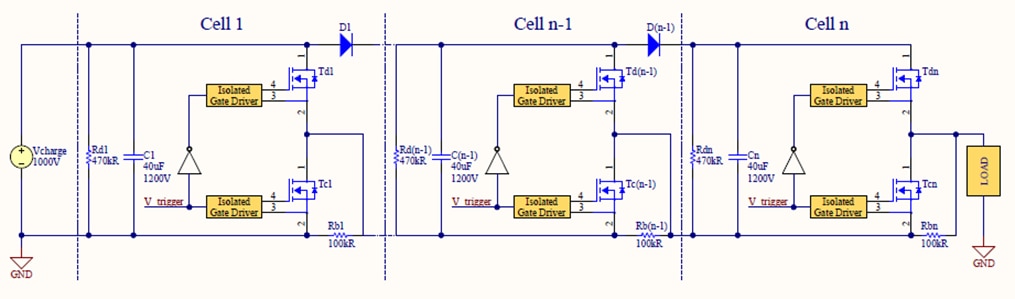
I'm designing a Marx generator with solid state switch. I'm using IGBTs.

Each IGBT has a 160uF capacitive load. At the moment I'm testing a generator that is powered with a 1kV and has 3 stages: the output voltage should be 3000V for a resistive load of 100Ohms.

Every stage of the marx is constituted by a half bridge with the gate isolated. Firstly I tested the same project with 6uF per stage and the system worked. When I try to discharge the Marx generator (with 160uF per cell) at the maximum voltage, I made the huge error to not connect any load. I heard a big burst and I noted that in one stage, the tracks of the half bridge were burned and the IGBT were faulted.

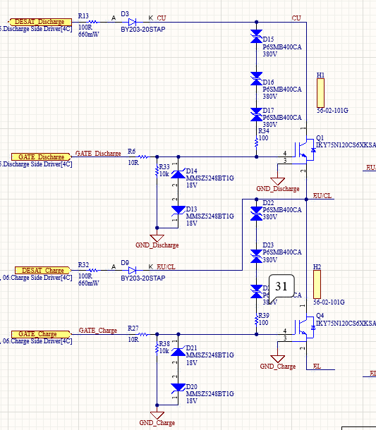
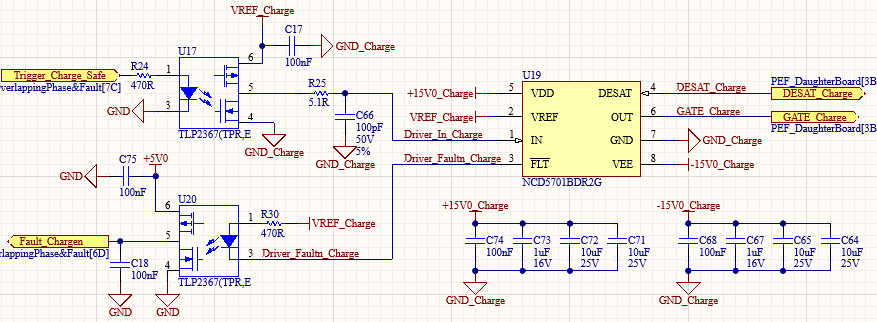
Apart from the huge mistake of not connecting the load, I'm thinking to protect the gate oh the high IGBT form the undesired switching on, due to floting voltage between the two IGBT. I saw in a marx generator (I am copying it in full) that there are a series of zener voltage and schottky diode between the gate and the emitter. Chat GPT says me that this should be a possible solution to avoid undesired switch on and protect the gate from overvoltage. It's not very clear for me how this could work.

Has anyone use it before? Any suggestion about the protection against undesired switching on for both IGBTs?

  • Sign in to reply
  • Cancel

Top Replies

  • michaelkellett
    michaelkellett 4 months ago +1
    How about posting a circuit and some pictures of your set up. MK
  • michaelkellett
    michaelkellett 4 months ago

    How about posting a circuit and some pictures of your set up.

    MK

    • Cancel
    • Vote Up +1 Vote Down
    • Sign in to reply
    • Cancel
  • finoconv
    finoconv 4 months ago in reply to michaelkellett

    Hi Michael, here is the final IGBT

    image

    And here is each gate driver stage

    image

    Here the layout and highlighted the burned tracks (they correspond to collector high, emitterhigh/collector low and emitter low)

    image

    Any suggestion will be precious.

    Thanks

    • Cancel
    • Vote Up 0 Vote Down
    • Sign in to reply
    • Cancel
  • dougw
    dougw 4 months ago

    Can you show a schematic? It sounds like you are not using a simple spark gap style Marx generator.

    • Cancel
    • Vote Up 0 Vote Down
    • Sign in to reply
    • Cancel
  • finoconv
    finoconv 4 months ago in reply to dougw

    I'm not using spark gaps. I'm using IGBT

    image

    here is the general schematic

    • Cancel
    • Vote Up 0 Vote Down
    • Sign in to reply
    • Cancel
  • dougw
    dougw 4 months ago in reply to finoconv

    What prevents "shoot through" (both transistors on at the same time)? The lower transistor turns on before the top transistor turns off.

    • Cancel
    • Vote Up 0 Vote Down
    • Sign in to reply
    • Cancel
  • michaelkellett
    michaelkellett 4 months ago in reply to finoconv

    Have you simulated this design ?

    Why use 2 IGBT per cell rather than one and a diode ?

    Are you connecting the IGBT gate drives to the drivers with long wires (the reason I asked for pictures is that it saves us having to ask these tedious questions).

    Doug's suggestion of shoot through sounds likely but I' wondering how we know that the 2 IGBTs are not both driven on.

    How many volts are you trying to generate and what is the purpose of this device.

    How many cells, was it the first one that burned out.

    You need to describe the issue comprehensively to have any hope of good advice.

    MK

    • Cancel
    • Vote Up 0 Vote Down
    • Sign in to reply
    • Cancel
  • finoconv
    finoconv 4 months ago in reply to michaelkellett

    this schematic is decriptive. in the top image you can see the gate driver stage.

    Marx generator needs two igbt, one for charging capacitor and one for discherging on the load during the erecting phase.

    Ihoot through is prevented since each rising edge of the gate signal is delayed by 6us but qhen there is no load, the floating voltage between two igbts doesn't discharge and this could cause hard switching (probabily).

    Anyway, my question is how to avoid undisered switching on on the high gate Slight smile

    • Cancel
    • Vote Up 0 Vote Down
    • Sign in to reply
    • Cancel
  • michaelkellett
    michaelkellett 4 months ago in reply to finoconv

    When you ask for help in a forum you are relying on others to expend time and thought on your problem. They are often willing to do so, but only under their own terms.

    My terms are that

    1) you are not trying to do something evil (but you won't say what this project is for)

    2) you are sharing the IP so I can learn from you

    You don't seem willing to play nicely so I shall leave you to solve your own problems.

    MK

    • Cancel
    • Vote Up 0 Vote Down
    • Sign in to reply
    • Cancel
  • finoconv
    finoconv 4 months ago in reply to michaelkellett

    Hi Michael, this marx generator are not for any evil, this will be used for food application trateing oil paste and crushed grapes to increare their organoleptic properties.

    I don't what you want to know. This is some simple half bridge in cascade, my question is about how to avoid undesired switching on in a half bridge :)

    • Cancel
    • Vote Up 0 Vote Down
    • Sign in to reply
    • Cancel
  • GaryGray
    GaryGray 3 months ago

    Hi finoconv,

    TLP2367 is made for 707V working insulation https://toshiba.semicon-storage.com/info/TLP2367_datasheet_en_20171025.pdf?did=36692&prodName=TLP2367

    (page 12  Viorm) in your 3rd stage the high driver insulation has to withstand 3000Vdc (2000Vdc for low side) !

    I can't see how the switch-on is delayed compared to the switching off (is there a diode missing in parallel to R6/R27  ;- )

    The protection diodes D15-17 P6SMB400CA need to supply 0,5A to drive against R6/R27 and the gate driver NCD5701 (no discharge diodes parallel R6/27 allowed, but you could have a gate discharge diode in series to R6/R27 and 100R in parallel to that diode ) !

    Actually the question is, what breakdown voltage are your IGBT rated? 1200V is not enough compared to your 400V suppressor diodes (Ir 1,5A -> Ur 500V) !

    I also would suggest to limit the 1000V Vsrc charging current, esp. if all three stages are switched low at the same time.

    The two gate protection Z-diodes could be replaced by one Zener and one or two shottkydiodes.

    Finally I don't see how the floating voltage of your Halfbridge-output should destroy your IGBT unless they have no body diodes, and I have no idea how this floating voltage should trigger your  High-driver unless your opto-insulator is not fit for his, sorry its job :- )

    Regards

    Gary

    PS: sorry for my bad english

    • Cancel
    • Vote Up 0 Vote Down
    • Sign in to reply
    • Cancel
element14 Community

element14 is the first online community specifically for engineers. Connect with your peers and get expert answers to your questions.

  • Members
  • Learn
  • Technologies
  • Challenges & Projects
  • Products
  • Store
  • About Us
  • Feedback & Support
  • FAQs
  • Terms of Use
  • Privacy Policy
  • Legal and Copyright Notices
  • Sitemap
  • Cookies

An Avnet Company © 2025 Premier Farnell Limited. All Rights Reserved.

Premier Farnell Ltd, registered in England and Wales (no 00876412), registered office: Farnell House, Forge Lane, Leeds LS12 2NE.

ICP 备案号 10220084.

Follow element14

  • X
  • Facebook
  • linkedin
  • YouTube