element14 Community
element14 Community
    Register Log In
  • Site
  • Search
  • Log In Register
  • Community Hub
    Community Hub
    • What's New on element14
    • Feedback and Support
    • Benefits of Membership
    • Personal Blogs
    • Members Area
    • Achievement Levels
  • Learn
    Learn
    • Ask an Expert
    • eBooks
    • element14 presents
    • Learning Center
    • Tech Spotlight
    • STEM Academy
    • Webinars, Training and Events
    • Learning Groups
  • Technologies
    Technologies
    • 3D Printing
    • FPGA
    • Industrial Automation
    • Internet of Things
    • Power & Energy
    • Sensors
    • Technology Groups
  • Challenges & Projects
    Challenges & Projects
    • Design Challenges
    • element14 presents Projects
    • Project14
    • Arduino Projects
    • Raspberry Pi Projects
    • Project Groups
  • Products
    Products
    • Arduino
    • Avnet Boards Community
    • Dev Tools
    • Manufacturers
    • Multicomp Pro
    • Product Groups
    • Raspberry Pi
    • RoadTests & Reviews
  • Store
    Store
    • Visit Your Store
    • Choose another store...
      • Europe
      •  Austria (German)
      •  Belgium (Dutch, French)
      •  Bulgaria (Bulgarian)
      •  Czech Republic (Czech)
      •  Denmark (Danish)
      •  Estonia (Estonian)
      •  Finland (Finnish)
      •  France (French)
      •  Germany (German)
      •  Hungary (Hungarian)
      •  Ireland
      •  Israel
      •  Italy (Italian)
      •  Latvia (Latvian)
      •  
      •  Lithuania (Lithuanian)
      •  Netherlands (Dutch)
      •  Norway (Norwegian)
      •  Poland (Polish)
      •  Portugal (Portuguese)
      •  Romania (Romanian)
      •  Russia (Russian)
      •  Slovakia (Slovak)
      •  Slovenia (Slovenian)
      •  Spain (Spanish)
      •  Sweden (Swedish)
      •  Switzerland(German, French)
      •  Turkey (Turkish)
      •  United Kingdom
      • Asia Pacific
      •  Australia
      •  China
      •  Hong Kong
      •  India
      •  Korea (Korean)
      •  Malaysia
      •  New Zealand
      •  Philippines
      •  Singapore
      •  Taiwan
      •  Thailand (Thai)
      • Americas
      •  Brazil (Portuguese)
      •  Canada
      •  Mexico (Spanish)
      •  United States
      Can't find the country/region you're looking for? Visit our export site or find a local distributor.
  • Translate
  • Profile
  • Settings
Test & Tools
  • Technologies
  • More
Test & Tools
Blog OpAmp basics: unbalanced to balanced signal with dual OpAmp
  • Blog
  • Forum
  • Documents
  • Files
  • Members
  • Mentions
  • Sub-Groups
  • Tags
  • More
  • Cancel
  • New
Join Test & Tools to participate - click to join for free!
  • Share
  • More
  • Cancel
Group Actions
  • Group RSS
  • More
  • Cancel
Engagement
  • Author Author: Jan Cumps
  • Date Created: 28 Aug 2022 4:32 PM Date Created
  • Views 12887 views
  • Likes 16 likes
  • Comments 13 comments
  • opamp
Related
Recommended

OpAmp basics: unbalanced to balanced signal with dual OpAmp

Jan Cumps
Jan Cumps
28 Aug 2022
OpAmp basics: unbalanced to balanced signal with dual OpAmp

A little OpAmp circuit to turn an unbalanced signal into a balanced one.
An unbalanced signal is the typical signal coming out of a signal generator, consumer audio equipment, headphone jacks.
A balanced signal uses two separate wires, with the same signal 180° inverted. It's used in RF, and professional audio equipment. It has some advantages, e.g. allows for less noise. But that's not the topic of this post.
What I show here is a common circuit to convert from unbal to bal.
image
I did this to test the little breakout board I made for a TI OPA2170. It's a dual OpAmp, and I wanted a neat circuit with two OpAmps to test it.

The circuit

I took an example from tina.com: 10. Amplifiers with balanced Inputs or Outputs.
image
source: tina.com Amplifiers with balanced Inputs or Outputs

It's a very simple circuit, where the output of the first OpAmp is identical to the input signal - but buffered. The second OpAmp is an inverting buffer and delivers the input signal, 180° phase shifted.
Together, these two signal form a buffered rendition of the input signal, with two times the amplitude.

I used a TI OPA2170 dual OpAmp. It's a low power device, with decent noise specs. Bandwidth up to 1.2 MHz. On the breakout board that I made, I soldered two 1 µF decoupling capacitors.
image
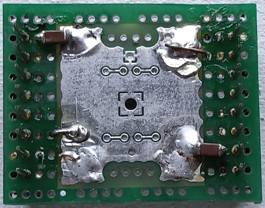
I used 5 10K resistors. One for the input, two in parallel for the 5K resistor, and the remaining ones for the two 10K resistors of the circuit.
This design is high impedance input. The input resistor can be made much higher than the 10K I used. In my case it wasn't critical. The unbalanced input comes from a function generator. So I just took the same value as all other resistors.

I built the circuit on a breadboard. Good enough in this case, where I use a 5 KHz signal.
image
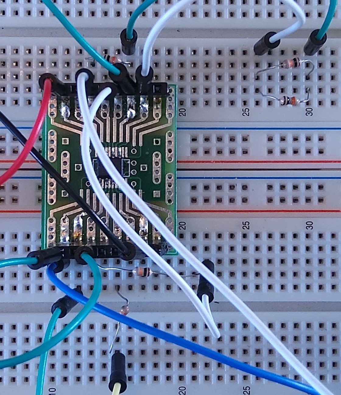
I used a balanced lab supply, set it to +9V / -9V. The function generator (the unbalanced source signal) is connected between ground and input, set to 5 KHz, 250 mVRMS, 0 V offset.

Probing a balanced signal

It's easy to probe an unbalanced signal. Connect the probe ground to ground, probe pin to the signal, and you have it.
A balanced signal runs over two wires, and none of these are ground. So you can't put your probe ground on one part, and probe pin on the other*.
A solution is to use two oscilloscope channels, and probe each of the two signals with one signal, as usual. Then use the oscilloscope's MATH function to show the difference of the two.
image
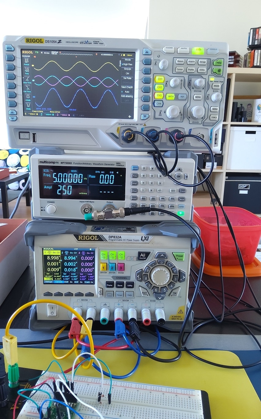
You see the result in the scope capture above. Channel 1 (yellow) is the unbalanced input - the signal coming out of the generator.
Channel 2 (cyan) the output of the left OpAmp. It's the bufffered input signal, and forms one part of the balanced output.
Channel 3 (magenta) is the output of the right OpAmp, and is the inverted component of the balanced output.
The difference between the two is the balanced signal. I used the Math (purple) difference (A - B: channel2 - channel 3) function to show it. Because both balanced halves have the same amplitude as the source - and are 180° inverted, the total balanced signal  has double the amplitude of the input.

One of the properties of a balanced signal is that the inversion removes noise. External noise will impact both components of the balances signal almost the same. When you then take the difference, identical noise on the lines cancels itself out, while the signal keeps its form. 

image

*you can. I leave it to fellow community members to put possibilities in the comments


  • Sign in to reply
  • Jan Cumps
    Jan Cumps over 2 years ago in reply to jc2048

    I did a naïve attempt - just build the single difference amp circuit and compare output to input.

    image

    • Cancel
    • Vote Up 0 Vote Down
    • Sign in to reply
    • More
    • Cancel
  • jc2048
    jc2048 over 2 years ago in reply to Jan Cumps

    Here's why parts are offered with closely matched resistors and why The Art Of... shows them to you.

    image
    This is the circuit twice, using the sim model for the op amp you chose. U1 has all the resistors exactly the same, U2 has one of the resistors, R8, out by 1%. Voltage sources VS3 and VS4 are each 0.5V and give 1V between the inputs at all times. I've got a voltage generator then sweeping the common point between them from -10V to +10V over 20 seconds (slow enough that there won't be any complications from dynamic effects). Ideally, the outputs will sit on 1V the whole time.

    Here is the result.

    image
    With the resistors perfectly matched, the output is out by 500uV, which is an offset error from the op amp, and there's a slight slope, which is the common-mode error contributed by the op amp. (If you needed the offset to be better, you could either test your op amps, to see if one was particularly good, or you could pay more for a superior one with better specs.)

    With the second circuit, you can see that there's a considerable problem with the common-mode error as it moves away from zero. (Although I didn't investigate it, I think that there will also be a problem if it's temperature cycled - essentially it's a form of bridge, but once the symmetry goes, the temperature variation in the resistances would now no longer cancel.)

    How much it's a problem depends on what you're doing with it. In your case, your driver outputs are individually referenced to ground, so it would work better for you than for situations where the common-mode voltage can move away from zero.

    • Cancel
    • Vote Up 0 Vote Down
    • Sign in to reply
    • More
    • Cancel
  • Jan Cumps
    Jan Cumps over 2 years ago in reply to jc2048

    The Art of Electronics runs this one too. With little explanation though (that's typical for that book).
    image

    tangent: the image above is taken from the book with a tablet camera, then filtered by Microsoft Lens. Almost as good as a flatbed scan.

    • Cancel
    • Vote Up 0 Vote Down
    • Sign in to reply
    • More
    • Cancel
  • jc2048
    jc2048 over 2 years ago in reply to Jan Cumps

    Who's making all that noise? You woke me up.

    A third possibility, for low frequencies and voltages, is to do your own differential input amplifier with an op amp. Something like this would get you started

    image

    That's from Analog Signal Processing by Ramon Pallas-Areny and John G. Webster. It's a nice book. I'm sure all the material in it could be found on-line, as application notes etc, if you knew where to look, but it's good to have it all collected together in a well-structured way. I wouldn't be able to justify the cost of the new book, now, but I got this one secondhand for a few pounds and for that it was an absolute bargain.

    The beautiful seed case is from a Hollyhock (Alcea).

    • Cancel
    • Vote Up 0 Vote Down
    • Sign in to reply
    • More
    • Cancel
  • Jan Cumps
    Jan Cumps over 2 years ago

    I leave it to fellow community members to put possibilities in the comments

    Alight. They are asleep.

    One alternative is to use a differential probe. This probe is isolated from ground.
    It can measure the signal between two test points that aren't ground.
    image
    I've attached the two inputs of the differential probe to the output of OpAmp A and B. Those are the points that are also probed by oscilloscope CH 2 and 3.
    In the capture you can see that the dark blue differential probe signal (oscilloscope CH 4) is virtually identical to the MATH signal (calculated difference between CH 2 and 3). But cleaner:
    image
    In the capture below, the original signal and the differential output are compared. The output has twice the amplitude of the input. In the capture they show with the same hight, because I set CH 1 to 500 mV/div and CH4 to 1 V/div.
    image


    • Cancel
    • Vote Up 0 Vote Down
    • Sign in to reply
    • More
    • Cancel
>
element14 Community

element14 is the first online community specifically for engineers. Connect with your peers and get expert answers to your questions.

  • Members
  • Learn
  • Technologies
  • Challenges & Projects
  • Products
  • Store
  • About Us
  • Feedback & Support
  • FAQs
  • Terms of Use
  • Privacy Policy
  • Legal and Copyright Notices
  • Sitemap
  • Cookies

An Avnet Company © 2025 Premier Farnell Limited. All Rights Reserved.

Premier Farnell Ltd, registered in England and Wales (no 00876412), registered office: Farnell House, Forge Lane, Leeds LS12 2NE.

ICP 备案号 10220084.

Follow element14

  • X
  • Facebook
  • linkedin
  • YouTube