element14 Community
element14 Community
    Register Log In
  • Site
  • Search
  • Log In Register
  • Community Hub
    Community Hub
    • What's New on element14
    • Feedback and Support
    • Benefits of Membership
    • Personal Blogs
    • Members Area
    • Achievement Levels
  • Learn
    Learn
    • Ask an Expert
    • eBooks
    • element14 presents
    • Learning Center
    • Tech Spotlight
    • STEM Academy
    • Webinars, Training and Events
    • Learning Groups
  • Technologies
    Technologies
    • 3D Printing
    • FPGA
    • Industrial Automation
    • Internet of Things
    • Power & Energy
    • Sensors
    • Technology Groups
  • Challenges & Projects
    Challenges & Projects
    • Design Challenges
    • element14 presents Projects
    • Project14
    • Arduino Projects
    • Raspberry Pi Projects
    • Project Groups
  • Products
    Products
    • Arduino
    • Avnet Boards Community
    • Dev Tools
    • Manufacturers
    • Multicomp Pro
    • Product Groups
    • Raspberry Pi
    • RoadTests & Reviews
  • About Us
  • Store
    Store
    • Visit Your Store
    • Choose another store...
      • Europe
      •  Austria (German)
      •  Belgium (Dutch, French)
      •  Bulgaria (Bulgarian)
      •  Czech Republic (Czech)
      •  Denmark (Danish)
      •  Estonia (Estonian)
      •  Finland (Finnish)
      •  France (French)
      •  Germany (German)
      •  Hungary (Hungarian)
      •  Ireland
      •  Israel
      •  Italy (Italian)
      •  Latvia (Latvian)
      •  
      •  Lithuania (Lithuanian)
      •  Netherlands (Dutch)
      •  Norway (Norwegian)
      •  Poland (Polish)
      •  Portugal (Portuguese)
      •  Romania (Romanian)
      •  Russia (Russian)
      •  Slovakia (Slovak)
      •  Slovenia (Slovenian)
      •  Spain (Spanish)
      •  Sweden (Swedish)
      •  Switzerland(German, French)
      •  Turkey (Turkish)
      •  United Kingdom
      • Asia Pacific
      •  Australia
      •  China
      •  Hong Kong
      •  India
      •  Korea (Korean)
      •  Malaysia
      •  New Zealand
      •  Philippines
      •  Singapore
      •  Taiwan
      •  Thailand (Thai)
      • Americas
      •  Brazil (Portuguese)
      •  Canada
      •  Mexico (Spanish)
      •  United States
      Can't find the country/region you're looking for? Visit our export site or find a local distributor.
  • Translate
  • Profile
  • Settings
Test & Tools
  • Technologies
  • More
Test & Tools
Blog Soldering Tiny Temperature Sensors
  • Blog
  • Forum
  • Documents
  • Files
  • Members
  • Mentions
  • Sub-Groups
  • Tags
  • More
  • Cancel
  • New
Join Test & Tools to participate - click to join for free!
  • Share
  • More
  • Cancel
Group Actions
  • Group RSS
  • More
  • Cancel
Engagement
  • Author Author: shabaz
  • Date Created: 24 Oct 2023 6:52 PM Date Created
  • Views 2028 views
  • Likes 11 likes
  • Comments 12 comments
  • soldering tips
  • sensirion
  • qfn
  • soldering station
  • soldering iron
  • soldering_tools
  • flux
Related
Recommended

Soldering Tiny Temperature Sensors

shabaz
shabaz
24 Oct 2023

I've been experimenting with temperature sensors, and really liked Sensirion products, since they are pretty accurate and reasonably low cost, and have a sensible board-level interface, I2C. However, they are quite small!

The good thing, is that they are not too difficult to solder by hand. This ultra-short blog post shows how I went about it.

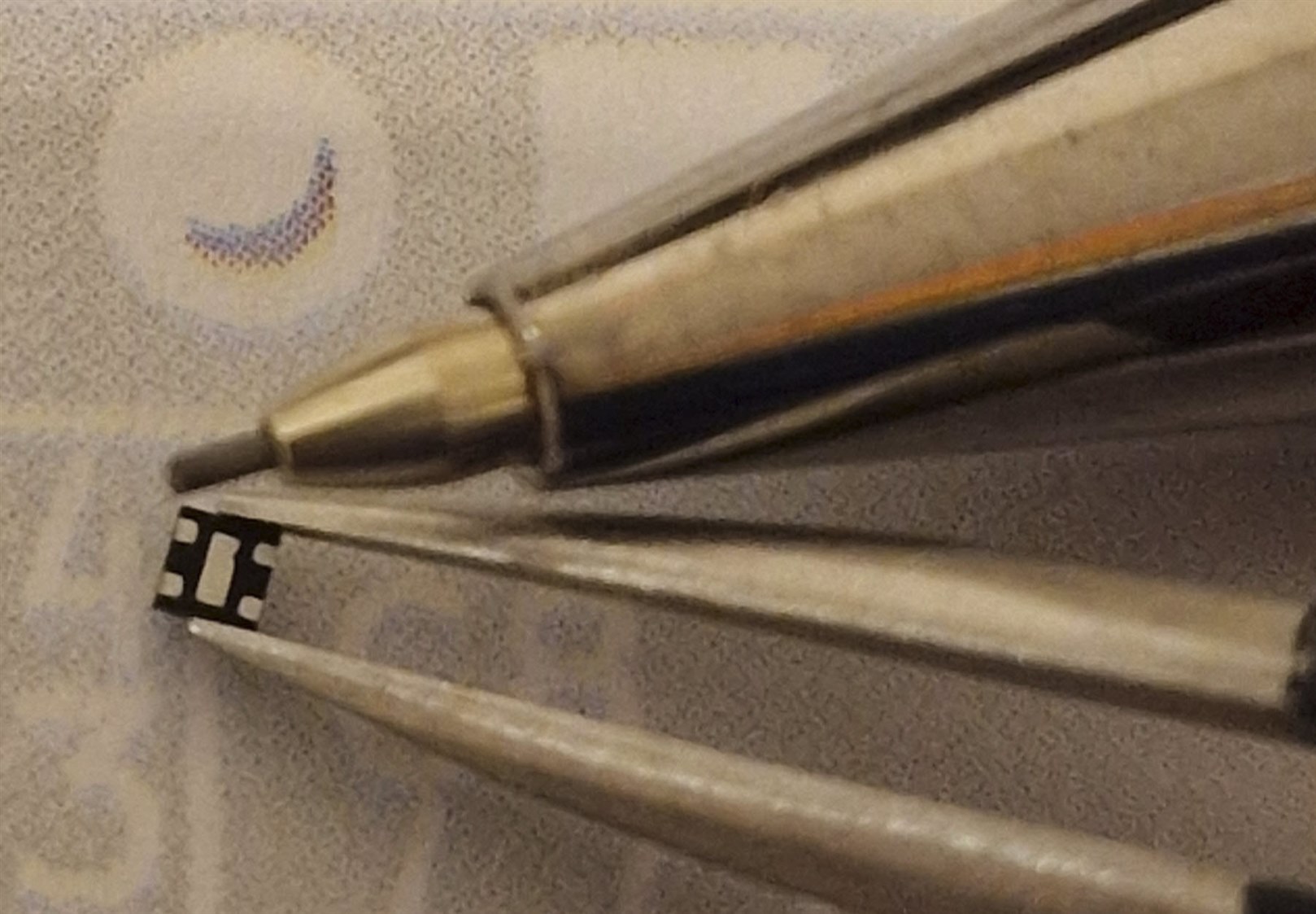
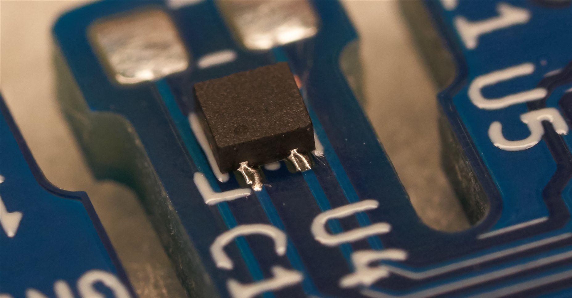
The part is 1.5 mm on its longest edge (i.e. it is smaller than the thickness of a normal PCB). The photo shows a 0.5 mm pencil for a size comparison.

So, first of all a decent pair of tweezers is needed, otherwise the part will go flying. Squared-end tweezers provide a lot of grip on the part, and it is a reliable way to manipulate the part. Good eyewear or a magnifier is needed to notice the tiny notch on the underside, which indicates pin 1 (there is a marking on the top side too). I used a mobile phone camera for this snapshot, and it was good enough to be sure of the part orientation.

image

I could have used a hot air tool, but I wanted to stick with a soldering iron for this exercise. First off, I applied flux paste to the four pads on the circuit board, which happened to have a small amount of solder already on it as manufactured (it's known as a HASL finish on the board). HASL isn't great, but it's cheap.

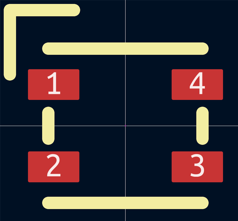
Another thing to pay attention to, is the component footprint. Unless you've got excellent eyesight or a microscope, you're going to be relying a lot on the silkscreen outline to align the part to the PCB. Therefore, it's quite important to have a decent silkscreen that is of the correct dimensions to match the part. In the screenshot below, since the part is 1.5 mm square, I made sure that the silkscreen was that size too (with a fraction of a millimeter exceeding the package size, so that I could place the part and still be able to see the outline an equal amount on all sides.

The pads were extended slightly, to suit the soldering iron method, since the iron tip needs to touch the pads.

image

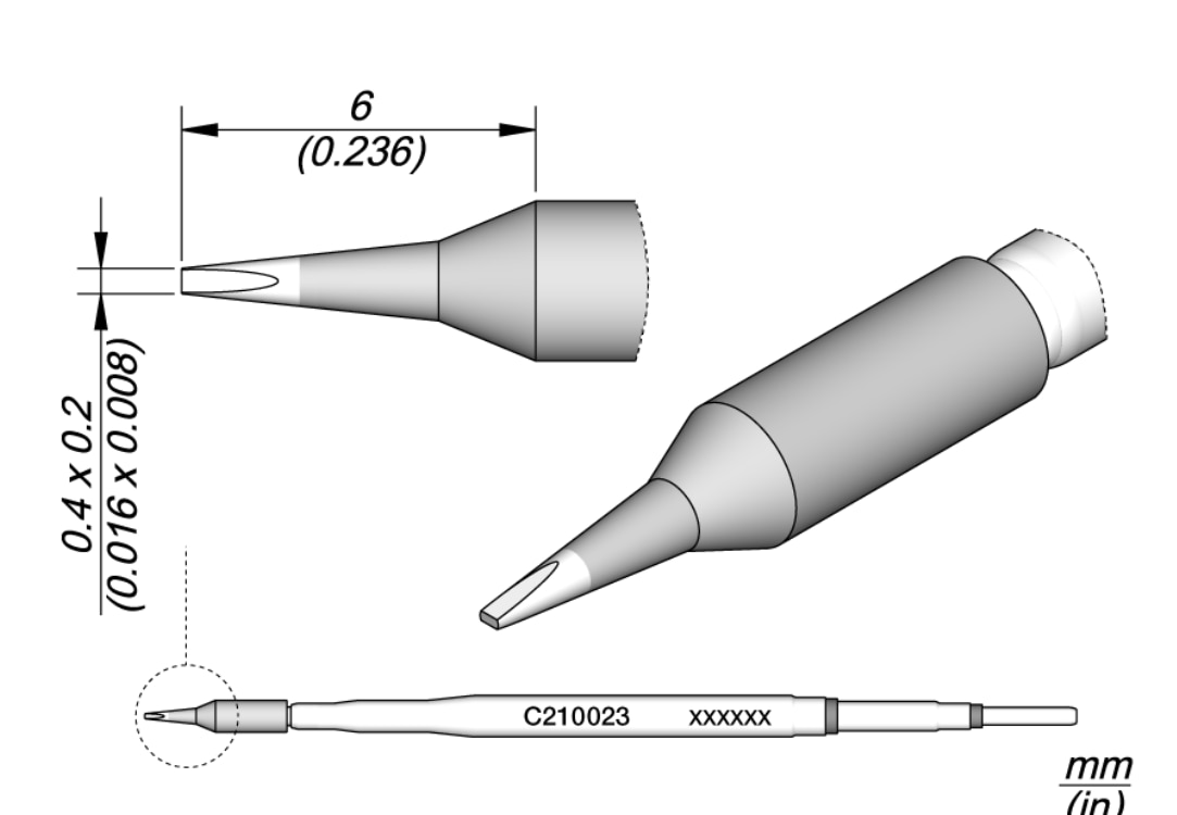
Speaking of soldering iron tips, for this scenario, a pointy tip works great, because it needs to get right into the corner between the component body and the pad. I used the tip shown in the drawing below, which to all intents and purposes is a pointy tip, since the dimensions of the end are so small (0.4 x 0.2 mm).

Any decent manufacturer soldering iron (JBC, Weller, etc) would work great, provided small tips are available. An integrated heater in the tip can make a good difference too. A low-cost soldering iron that uses tips with integrated heaters is the Secure S60; it supports such small dimension tips, and also works with larger tips for more normal soldering too. Note that if you're using a USB soldering iron, then it needs to be grounded when soldering semiconductors.

image

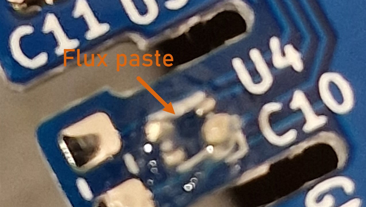
As mentioned, I splurged some flux paste onto the pads. Apologies for the photo quality, it was done with a shaky mobile phone. There's not much to see anyway, it's just flux. At these dimensions, the flux paste will be a single blob, it won't be precisely dispensed just on the pads.

image

The flux paste was called MG Chemicals 8341 others would be fine too, I'm just used to using that stuff so I stuck with what works.

Next, the part was oriented correctly and placed inside the silkscreen box shape with the tweezers, flat against the board. With the other hand, the soldering iron (with a small amount of solder on the tip was dabbed into the corner to touch the pads and the side of the component. Surface tension allowed the metal parts to retain just enough solder for a nice fillet, although really you're flying blind at this point, because the flux covers your view. Anyway, you can trust science at this point, and just dab in the general corner areas. 

Once that's done, the board is cleaned. I used isopropyl alcohol and a brush (it is very expensive for a brush, but it is brilliant, and will last for a decade or longer). The cheap brushes on Amazon are hopeless compared to that one, and then I used a wipe to mop things up.

Finally, the fillets of solder need to be inspected. You could use a mobile phone camera if nothing else is handy. I used a normal camera here:

image

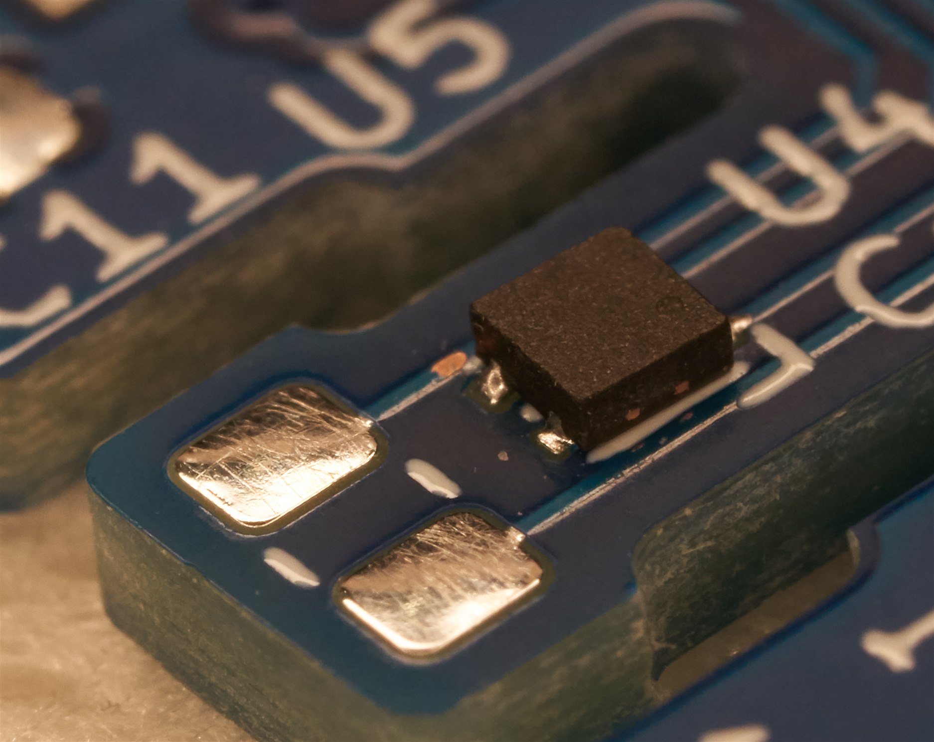
As you can see, it's a bit wonky, but nevertheless all the pads are soldered with no shorts, and that's all that matters for this part. 

image

Summary

With not a lot of effort or cost, it is feasible to solder quite tiny parts, relying on surface tension and flux to manage the distribution of solder with no short circuits. Still, a fairly decent soldering iron and tip is needed, but they are not necessarily expensive these days. Particularly for a temperature sensor, you might want low thermal mass, and so using a small part might make the difference between merely an adequate solution or a (hopefully) better performing one. 

Thanks for reading!

  • Sign in to reply

Top Comments

  • genebren
    genebren over 1 year ago +1
    Nicely done! I noticed that the silk screening on the PCB might be slightly lifting the component. I find that on some tiny parts, I either leave off the component outline or enlarge it sufficiently…
Parents
  • genebren
    genebren over 1 year ago

    Nicely done!

    I noticed that the silk screening on the PCB might be slightly lifting the component.  I find that on some tiny parts, I either leave off the component outline or enlarge it sufficiently keep it from allowing the part to drop through and make good contact to the PCB.

    • Cancel
    • Vote Up +1 Vote Down
    • Sign in to reply
    • More
    • Cancel
Comment
  • genebren
    genebren over 1 year ago

    Nicely done!

    I noticed that the silk screening on the PCB might be slightly lifting the component.  I find that on some tiny parts, I either leave off the component outline or enlarge it sufficiently keep it from allowing the part to drop through and make good contact to the PCB.

    • Cancel
    • Vote Up +1 Vote Down
    • Sign in to reply
    • More
    • Cancel
Children
  • shabaz
    shabaz over 1 year ago in reply to genebren

    Hi Gene, 

    Thanks!

    I think there's an element of that occurring, but for hand-soldering I figured that was better than not having any outline, since it's very hard to align and hold in place a 1.5 mm part without any surrounding visual reference. Good point that it could be slightly larger. In the past the silkscreen had enough inaccuracy that even if it's slightly larger, since it's still sub-millimeter, one edge may touch (unless it's spaced out a lot, which is common with machine-placed parts). But from visual inspection, these boards seem to have an excellent silkscreen

    • Cancel
    • Vote Up 0 Vote Down
    • Sign in to reply
    • More
    • Cancel
element14 Community

element14 is the first online community specifically for engineers. Connect with your peers and get expert answers to your questions.

  • Members
  • Learn
  • Technologies
  • Challenges & Projects
  • Products
  • Store
  • About Us
  • Feedback & Support
  • FAQs
  • Terms of Use
  • Privacy Policy
  • Legal and Copyright Notices
  • Sitemap
  • Cookies

An Avnet Company © 2025 Premier Farnell Limited. All Rights Reserved.

Premier Farnell Ltd, registered in England and Wales (no 00876412), registered office: Farnell House, Forge Lane, Leeds LS12 2NE.

ICP 备案号 10220084.

Follow element14

  • X
  • Facebook
  • linkedin
  • YouTube