


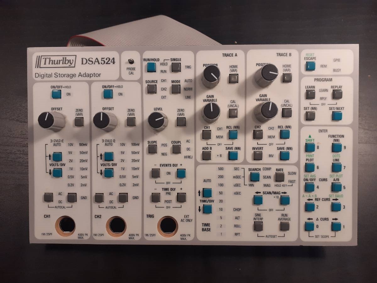
My curiosity got the better of me and I decided to take apart the Thurlby DSA524. This device is basically a Digital Storage Oscilloscope, without the oscilloscope part, that outputs an analog signal that let you use an old analog oscilloscope as a display. The captured waveforms can also be printed using an X-Y plotter or downloaded to a PC using the serial port or optional GPIB-port.
When looking at the boards it struck me that all the ICs inside seemed to be off-the-shelf components, most of which are logic gates along with a few OP-amps. Notably the analog section in particular make good use of the high input impedance and high voltage rating of 4000-series CMOS chips, while the digital section use 74-series gates for their higher speeds.
The circuits inside the device are an interesting combination of discrete transistor circuits along with integrated circuits, perhaps adapting proven designs or optimizing for cost? The date codes on the ICs seems to indicate that the unit was manufactured sometime in the second half of 1988.

The device is housed inside an off-the-shelf enclosure that’s been given custom-made aluminum panels. After removing the top the insides lifts straight up, with only a ground wire holding it to the shielded bottom plate.
To bring some order to this blog I divided it into sections, feel free to skip to the part of the teardown you’re most interested in.
Mechanical construction


The boards are neatly stacked and come out of the case in one piece along with the front and back panels. The front panels are both secured to the middle ground shield between the digital and analog sections. There’s a black ground strap hanging from the bottom that screws down into the shielding for the underside of the analog board. This wasn’t meant to be unscrewed, instead it’s one of three ground connections that has to be desoldered from the analog board when dissembling it.
Analog plotter interface
This expansion card is the first one in the stack of boards, and it’s used to drive an analog X-Y plotter to print waveforms.
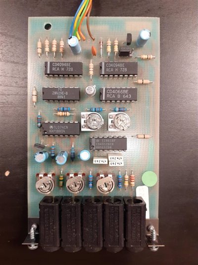
The card outputs X, YA and YB analog signals along with a digital Pen Lift signal. The inputs to the card are +/- 5 Volt and ground, along with Clock and Data. The data line and clock signal load bits into two 4094 8-stage parallel output shift-registers that are daisy-chained in series.
The first 4094 shift-register is used to set the digital inputs of the ZN429E-8 8-bit R-2R DAC. The voltage reference for the DAC is a ZN404 2.45 Volt precision reference regulator (the metal can next to it).
The second 4094 controls the switches in a 4066 quad analog switch. This switch is used for the Y signal where it switches two different series resistor and trimpot circuits. One of these circuits pull the line to Vref and the another towards ground. I'm not sure if this is used to attenuate the signal or for level shifting.
The second 4094 is also used to control the addressing of a 4052 dual 1 to 4 analog demultiplexer. The Y signal input is buffered by an OP-amp before it goes into the first half of the demux. While the X signal goes directly into the second half of the demux. Each of the three analog signals X, YA and YB are buffered by the TL074CNTL074CN quad OP-amp.
The three white 47nF polymer capacitors (under the 4052 demultiplexer) are connected between ground and the positive input on of the three output buffer OP-amps. It’s possible that these are part of a sample & hold circuit together with the demux, which would be used to hold the output voltages steady while the others signals are changed.
Digital section
The digital section is laid out on a 4 layer PCB and its heart is a HD6303RP 8-bit microprocessor, which has peripherals and a bit of RAM built in. This microprocessor is object-code upward compatible with the classic 6800 line of microprocessors.
The 65C22 VIA chip in the middle of this board is responsible for reading and writing to the many shift registers found throughout this unit. It does so by clocking only one of seven shift register clock lines at the time, each going to a different part of the circuit.
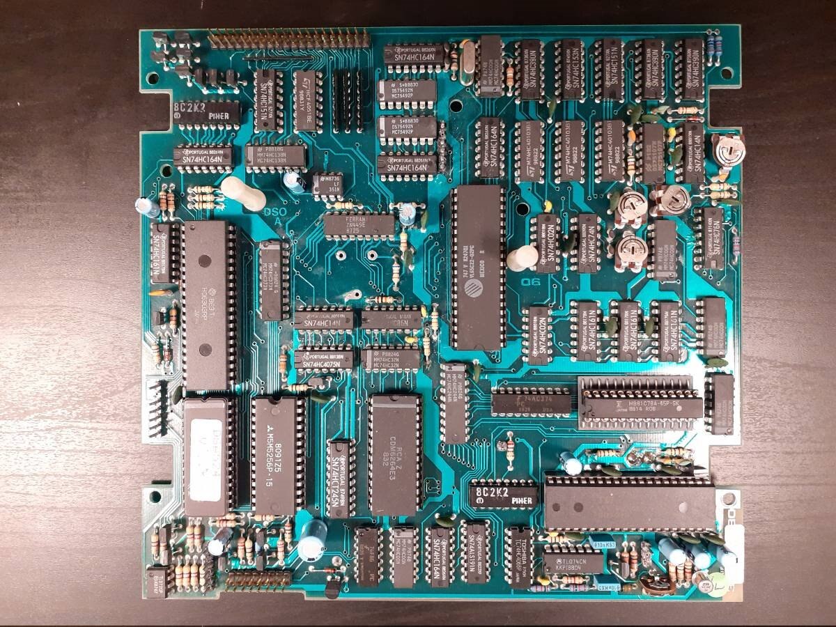
The main ADC is the big 40-pin DIP in the bottom right corner, a UVC3120 8-bit flash type analog to digital converter that also has an R-2R type DAC built in.
Missing from this board is a big Ni-MH cell that was used to hold settings, waveforms and button press sequences in RAM when the unit is off. This cell was removed to prevent further damage to the board.
Time base and ADC clock

The microprocessor is not fast enough to do the sampling at 20 MS/s, instead it triggers counters and discrete logic that handles the acquisition. The acquired waveform is stored in a separate SRAM memory where the microprocessor can access it.
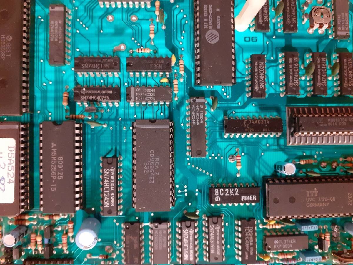
The 20 MHz timebase used for everything on the digital board is marked in yellow, along with its clock divider stages and clock frequency selectors. The 20 MHz clock comes from the oscillator made up of a 20 MHz crystal and a 74HC00 quad NAND gate. This 20 MHz clock is also divided down in stages by three 74HC390 dual decade ripple counters, so that the desired clock frequency can be selected using the 74HC153 dual 4-input multiplexer and 74HC151 8-bit multiplexer.
The ADC clock circuit is marked in brown. This clock is derived from the carry out signal of the 74HC40103 8-bit synchronous down counter, gated by a 74HC02 quad NOR gate and also fed into a 74HC74 dual D-type flip-flop.
RAM addressing, trigger delay and ADC voltage reference
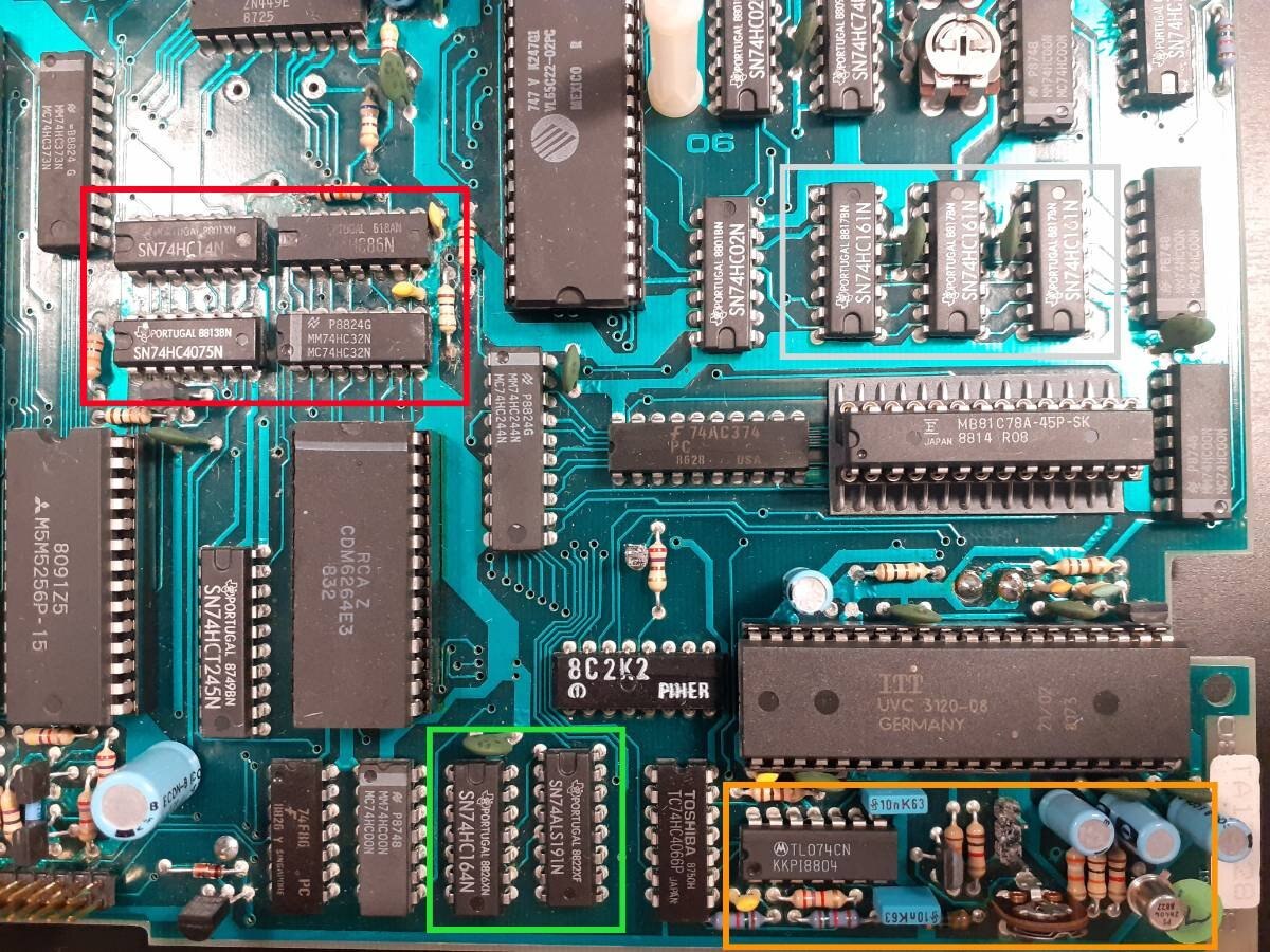
The trigger delay circuit is marked in green. In this circuit the desired delay is loaded into the 74HC164 8-bit parallel output shift register, which loads it into the 74ALS191 synchronous 4-bit up/down binary counter. This counter is then clocked by the trigger circuit.
The ADC’s voltage reference circuit is marked in orange. This circuit get its reference voltage from the ZN404 2.45 Volt precision reference regulator, which is buffered by the TL074 quad OP-amp.
The RAM paging circuit that provides paging between the ROM and RAMs is marked in red (there are no less than three SRAMs in this device). Under it is the M5M5256P 32K x 8-bit SRAM used for the display memory. The paging circuit is made up of a 74HC14 hex inverter, 74HC86 quad XOR gate, 74HC4075 triple 3-input OR gate and 74HC32 quad OR gate. The purpose of this circuit is to page out the ROM and RAM from memory during ADC acquisition RAM write cycles, to make sure that the ADC timing isn’t messed up.
The three 74HC161 presettable synchronous 4-bit binary counters marked in grey make up the ADC acquisition RAM address counter. The clock the address counter come from the 74HC40103 8-bit counter that we saw previously in the ADC clock circuit.
The long narrow MB81C78A chip mounted in an adapter is the high speed 8K x 8-bit SRAM used as acquisition memory. The 74AC374 octal D-type flip-flop next to it isolates the ADC from the RAM, presumably when the microprocessor is reading from it.
Shift register clock routing and front panel control

The 74HC138 3-to-8 line decoder marked in purple is used to route the shift register clock signals generated by the 65C22 VIA around the device. This is effectively substituting for a missing chip select pin on the shift registers.
The three 74HC164 8-bit parallel output shift registers marked in blue are used to drive the front panel LEDs, using the two DS75492 MOS-to-LED hex drivers and the transistors in the top-left corner. The front panel is arranged in a matrix and the shift registers act like column and row drivers. The 74HC151 8-bit multiplexer marked in white is used to read the buttons on the front panel, while the button press scanning is done in software.
The 4051 8-channel analog demultiplexer marked in pink is used to expand the ZN449E 8-bit SAR ADC to eight inputs, enabling the microprocessor to read each of the seven front panel potentiometers individually.
Analog Section
The analog section is laid out on a 2 layer PCB and contains the linear power supplies, the two oscilloscope input channels, the trigger input and two different sample & hold circuits.

The software running on the microprocessor does all the controlling of the input sections. In the middle of this board is the logic that’s used to send the control signals around the analog section.
Oscilloscope input section

The very first thing after the BNC input jack is a passive attenuator network that’s switched by relays for the x1, x10 and x100 attenuation. There’s also an AC-coupling capacitor that’s shorted out by a relay for DC-coupled signals and another relay that’s used to ground the input signal.
The attenuator stage is followed by a high-impedance input buffer stage where the signal is both AC-coupled into a J309 JFET transistor for the high frequency path, and DC-coupled into a LF351 JFET input OP-amp for the DC path. The two paths have filtering to obtain a flat frequency response when combined.
There is then another attenuation step after the buffer amplifier stage for the x2.5 and x5 attenuation. This stage uses transistors to controls a resistive voltage divider with frequency compensating capacitors.
The only IC in the input stage is an μA733 video amplifier with differential inputs and differential outputs. This amplifier is used to compensate for the DC-voltage offsets introduced by the previous stages. The DC-offset error is found by grounding the input and the correction voltage is generated from a DAC.
The main amplifier is after the differential amplifier and is made out discrete high speed PNP transistors. After the amplifier there’s a last attenuation stage made out of transistors acting as potential dividers for the 5, 10 and 20 mV ranges.
Trigger input

The external trigger amplifier is based on a JFET and is only one of the inputs to the trigger amplifier. The different input signals to the trigger amplifier are selected using NPN transistors. After the trigger amplifier there are impedance matching transistors and a voltage level shifting circuits, which forces the trigger signal to remain positive above analog ground. This signal then goes into the only IC in the trigger input section, a DS75107N dual line receiver, of which half is used for comparing the trigger signal to a trigger level reference.
The second half of the line receiver is used for the 50 Hz (mains frequency) trigger source. The 50 Hz trigger signal is obtained from a couple of rectifier diodes in the power supply, a sinewave, that’s then converted into a pulse by the line receiver for the trigger circuit.
DC-coupling is enabled by a transistor across the AC-coupling capacitor.
Sample & hold circuit(s) and control voltages

The three 4094 8-stage parallel output shift-registers marked in yellow are used to control the attenuation for both channels and to select the trigger source. The 4052 analog demultiplexer marked in orange controls the final attenuation for the 5, 10 and 20 mV ranges of CH1, while the 4052 marked in brown controls the lower attenuation settings.
The big white 160 nF polymer capacitors are part of a sample & hold circuit that’s used to supply control voltages to the input stages. The two 4052 demultiplexers (marked in orange and brown) together with the 4051 demux (marked in red) are used to connect these capacitors to an input voltage coming from a DAC on the digital board. Two of the OP-amps in the TL074 (to the left of the white caps) are used for comparing the sampled and held DAC voltages with a reference voltage. The difference between the two is fed into the differential amplifier in the input stage that's used to correct for the DC-offset error.
Two 74HC4066 quad analog switches marked in purple make up another sample & hold circuit, together with the green topped 22nF ceramic capacitors just below them. This circuit is used for sampling the two channels, or either channel, before sending it onto the ADC on the digital board. This is how a two channel oscilloscope was constructed from a single input ADC. At this point the waveform signals are level shifted into the ADC's input range so the faster 74HC logic can be used.
Power supply
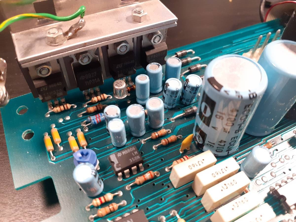
The power supply section provides four stabilized rails: +/- 7 Volt and +/- 5 Volt. The negative 5 Volt supply is generated using a regular 7905 regulator IC, while the other rails are generated using series regulators and OP-amps for the feedback loop (OP-amps controlling series pass transistor). The voltage references for all three series regulators comes from a ZN404 2.45 Volt precision reference regulator (the metal can next to the big transistors). The LM358 dual OP-amp in the picture is used for the +/- 7 Volt supply feedback loops and out of frame is a TL072 that's used for the positive 5 Volt supply.
Front panel
The front panel is just a passive board wired up in a matrix for the status LEDs and another for the buttons. The seven potentiometers on the front panel are connected to an 8 to 1 multiplexer that's feeding into an ADC.
Closing words
While I ended up spending a lot more time that I had planed on trying to decipher my Xerox copy of the service manual, I did still find this to be a very enjoyable teardown. I think the use of shift registers throughout this device is neat and that the shift register clock multiplexing is a clever solution. So while I was hoping to do a project with this device, I can only conclude that it's so tightly integrated with its software that it's best to let it be.
If you're interested, check my blog index for my other teardown blogs.
Top Comments