element14 Community
element14 Community
    Register Log In
  • Site
  • Search
  • Log In Register
  • About Us
  • Community Hub
    Community Hub
    • What's New on element14
    • Feedback and Support
    • Benefits of Membership
    • Personal Blogs
    • Members Area
    • Achievement Levels
  • Learn
    Learn
    • Ask an Expert
    • eBooks
    • element14 presents
    • Learning Center
    • Tech Spotlight
    • STEM Academy
    • Webinars, Training and Events
    • Learning Groups
  • Technologies
    Technologies
    • 3D Printing
    • FPGA
    • Industrial Automation
    • Internet of Things
    • Power & Energy
    • Sensors
    • Technology Groups
  • Challenges & Projects
    Challenges & Projects
    • Design Challenges
    • element14 presents Projects
    • Project14
    • Arduino Projects
    • Raspberry Pi Projects
    • Project Groups
  • Products
    Products
    • Arduino
    • Avnet Boards Community
    • Dev Tools
    • Manufacturers
    • Multicomp Pro
    • Product Groups
    • Raspberry Pi
    • RoadTests & Reviews
  • Store
    Store
    • Visit Your Store
    • Choose another store...
      • Europe
      •  Austria (German)
      •  Belgium (Dutch, French)
      •  Bulgaria (Bulgarian)
      •  Czech Republic (Czech)
      •  Denmark (Danish)
      •  Estonia (Estonian)
      •  Finland (Finnish)
      •  France (French)
      •  Germany (German)
      •  Hungary (Hungarian)
      •  Ireland
      •  Israel
      •  Italy (Italian)
      •  Latvia (Latvian)
      •  
      •  Lithuania (Lithuanian)
      •  Netherlands (Dutch)
      •  Norway (Norwegian)
      •  Poland (Polish)
      •  Portugal (Portuguese)
      •  Romania (Romanian)
      •  Russia (Russian)
      •  Slovakia (Slovak)
      •  Slovenia (Slovenian)
      •  Spain (Spanish)
      •  Sweden (Swedish)
      •  Switzerland(German, French)
      •  Turkey (Turkish)
      •  United Kingdom
      • Asia Pacific
      •  Australia
      •  China
      •  Hong Kong
      •  India
      •  Korea (Korean)
      •  Malaysia
      •  New Zealand
      •  Philippines
      •  Singapore
      •  Taiwan
      •  Thailand (Thai)
      • Americas
      •  Brazil (Portuguese)
      •  Canada
      •  Mexico (Spanish)
      •  United States
      Can't find the country/region you're looking for? Visit our export site or find a local distributor.
  • Translate
  • Profile
  • Settings
Test & Tools
  • Technologies
  • More
Test & Tools
Forum Simple Electronic DC Load Conditional Oscillations
  • Blog
  • Forum
  • Documents
  • Files
  • Members
  • Mentions
  • Sub-Groups
  • Tags
  • More
  • Cancel
  • New
Join Test & Tools to participate - click to join for free!
Actions
  • Share
  • More
  • Cancel
Forum Thread Details
  • State Verified Answer
  • Replies 30 replies
  • Answers 18 answers
  • Subscribers 358 subscribers
  • Views 5644 views
  • Users 0 members are here
  • electronic_dc_load
Related

Simple Electronic DC Load Conditional Oscillations

jw0752
jw0752 over 7 years ago

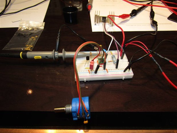
I have recently completed a build of a simple DC electronic load with the specifications of 1 mA to 2000 ma and up to 55 Volts as long as total power is kept below 60 Watts. I will be blogging about this build in the coming days.


During the prototyping phase of the project I had no problems with oscillations but moving the design to a circuit board always has the potential to change things. In this case I find that the unit works properly if I bring up the load from a low current to the desired level or if I bring the voltage applied to the load from a low level up to the desired voltage. If however I have the load set for any value over 250 mA and then apply a voltage above 6 volts I will get an oscillation that is undesirable. Once the unit is powered and free of oscillation I am able to move the voltage to any level and the load to any level without any recurrence of the oscillation. It seems that it is just the initial impact of full voltage into a previously set load that is greater than 250 mA that triggers the oscillation.


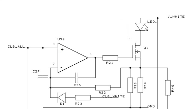
Now it is very possible that the design that I have used, which has a general traditional layout with my own modifications frankensteined into it, is bad. Since I am not an engineer I can do things like this but if I fail then I need the engineers to help me clean up my mess. Here is a schematic of the project and any insights on how I can make the unit oscillation proof will be welcome.


image

Since this is just a tool for my own shop I can live with the oscillation anomaly as the power or the load can just routinely be brought together gently but aesthetically it would be nice if it didn't have to be babied.


Thanks John

  • Sign in to reply
  • Cancel

Top Replies

  • hlipka
    hlipka over 7 years ago in reply to jw0752 +8 verified
    Things to notice: the LT1006 is not a rail-to-rail opamp. With 5V suppy its output goes up to between 4.0 and 4.4V (best case), depending on the load, which is not enough to ensure the IRF234 is fully…
  • hlipka
    hlipka over 7 years ago in reply to jw0752 +7 suggested
    Using a R2R-Opamp only solves part of the problem. When looking at the data sheet for the IRF234, especially at the diagram 'drain current vs. gate voltage', you see that even at 5V gate voltage only 1A…
  • hlipka
    hlipka over 7 years ago +6 suggested
    I cannot see the image (and directly using its URL says 'no permission'). One change that happens between a breadboard and a PCB is that on a breadboard usually the parasitic capacities are higher. This…
Parents
  • jadew
    0 jadew over 7 years ago

    Hey John,


    Don't know how far you've gotten with your redesign, but there are a couple of things I would change in the first one:


    1). I'd get rid of the first op amp (edit: also of R2 and R3). A 6-7k resistor, in series with the 10k pot, will make the output of the potentiometer be exactly what it is on the positive input of U2. Since C3 will still be there (hopefully a bit smaller), your set point will be much more stable than it is coming out of U1. This won't solve your problems, but it should be an improvement.


    2). Get rid of R6, like the others have said, but also of C4. You want as little capacitance and filtering as possible in the feedback path.


    3). If after removing R6 and C4 you're still having issues, you can try slowing down the output, so a snubber network might be in order on the output of the op amp, or you could add a small cap from the output of the op amp, before R4 to the negative input.


    Edit: Oups, the 6-7k resistor should be only 4.5k.


    Regards,

    Razvan

    • Cancel
    • Vote Up +5 Vote Down
    • Sign in to reply
    • Verify Answer
    • Reject Answer
    • Cancel
  • jw0752
    0 jw0752 over 7 years ago in reply to jadew

    Hi Razvan,


    Thank you for the good ideas to improve the design. I will eliminate the buffer op amp and set up the resistor divider to deliver the proper voltage to pin 2 of the driver Op Amp. In this case I want 2 volts as this will give me a corresponding 2 Amp max load. R6 will be eliminated and I still have to figure out how I am going to continue to implement the changes as suggested by Hendrik and you until I understand this circuit better. Unfortunately I am now working on a solder PCB and not the bread board and changing out parts for experiments is quite a bit more difficult. I won't be able to complete the experiments until tonight but the good advice I have received gets me steadily closer to a good resolution.


    John

    • Cancel
    • Vote Up +6 Vote Down
    • Sign in to reply
    • Verify Answer
    • Reject Answer
    • Cancel
  • michaelkellett
    0 michaelkellett over 7 years ago in reply to jw0752

    Hello John,


    Here is an LED current driver. I've used variations of this circuit in many designs and there are hundreds of thousands of them in the field. (Mostly working OK, I guess, since the customer is still with me !).


    image


    This one is a little odd since it came from a design that I can publish. The concept is very similar to Razvan's excellent suggestions.

    The transient response (and in extremis; stopping oscillating) is tuned by the combination of MOSFET gate rapacity, R21, R22 and C26. Good starting values are C26 =  220pF and  R21 = 560R, R22 = 4k7.

    This design used pulse width modulation with logic pulses applied to the CL0_WHITE net (3.3V applied = no output current). You might want to keep this as an emergency stop, or even as a way of checking transient response of things you are testing.

    R20 and R36 are the current sense resistors (I used 2 because 2 x 1R were much cheaper than 1 x 0.5R).

    The current is set by the voltage on the CL0_ALL net.

    If you want a current of 2A max I suggest you set the current sense resistor to 0.22 ohms. Now you will need 0.44 V max.

    If you use a nice modern op amp like OPA192 with a 10V op amp supply you will be able to drive the MOSFET full on but the low offset voltage of the OPA192 (25uV max at 25C) will only result in a zero error current of 113uA which seems OK.

    You'll need to pot down the signal from your current control from 0 - 3.3V to 0 - 0.44V.

    If the modulation pin is to be able to turn the MOSFET off with maximum current demand and 3.3V applied R23/(3.3 - 0.6 - 0.5) = R22/0.5, so R23 = 4.4 * R22. For R22 = 4K7 use 20k for R23.

    R40 was for current monitoring and went off to an ADC.


    You can simulate how this will work quite well using (free) TINA from TI.

    If you can't get the OPA192 almost any 10V rail to rail CMOS op amp would do but most will have much worse offset voltages.


    MK

    • Cancel
    • Vote Up +4 Vote Down
    • Sign in to reply
    • Verify Answer
    • Reject Answer
    • Cancel
  • jw0752
    0 jw0752 over 7 years ago in reply to michaelkellett

    Hi Michael,


    Thank you for taking the time to share the design with me. I will check out the OPA192 Op amp as it sounds like a very useful one. The oscillation problem is going to force me to learn more about this subject than I intended so it is good. Thankfully I always get such great response and insights from my friends.


    John

    • Cancel
    • Vote Up +2 Vote Down
    • Sign in to reply
    • Verify Answer
    • Cancel
  • jw0752
    0 jw0752 over 6 years ago in reply to michaelkellett

    Hi Michael, Jon, Frank, Razvan, and Hendrik,


    I want you to know that your suggestions are not wasted on me. Since I last posted on this discussion I have ordered in some OPA 192 Op Amps, Some of the TI SO 8 adapter boards and I have gone back to bread boarding and experimenting with your suggestions. I wanted to get a design that used good Op Amp practices and was stable over the desired current and voltage ranges. I began my redesign by changing the reference voltage section to use a TL431 at its lowest setting 2.5 Volts. The application of this voltage to pin 3 of the OPA192 was controlled by a 10K 10T potentiometer. The resistance of R3 was lowered to 47 Ohms. I began my testing with a direct connection between the sense resistor and pin 2 of the OPA but I found that I got oscillations at low input voltages and moderate 500 mA to 1 A currents. While I hadn't seen a resistor in the connection between the sense resistor and pin 2 there was one in Michaels recommended circuit. When I put a 4K7 between the sense resistor and the pin 2 of the OPA192 I saw an immediate improvement in the performance of the circuit. I next moved on to the small capacitor between the OPA output pin 6 and pin 2. I began at 30 pF which also improved performance. This was gradually increased to 200 pF (which was a recommended value). At 200 pF the circuit remained stable over the entire test range. With the excellent suggestions I feel that I have simplified the circuit and feel very good about its stability.


    Michael if you can tell me what is the reason and side effect of the 4K7 at R2 it would be appreciated.


    Frank, just a side note. I am used to using Chinese adapter boards and I found the TI boards to be much better quality. However, I had just mounted 16 SO-8 chips onto Chinese boards in the last couple days so I was very used to their orientation and true to my form I didn't look carefully before I orientated the OPA 192 on the TI adapter board. The TI adapter is 180 degrees different from the Chinese boards. Of course I got it on backwards !!  Fortunately I was able to scrape off the two pin numbers and redesignate pin 1 with some white paint.


    Here is my bench test set up for this experiment and a copy of the schematic for the best circuit design so far.


    image


    image

    Thanks to everyone, hopefully I haven't beat this topic to death yet.


    John

    • Cancel
    • Vote Up +3 Vote Down
    • Sign in to reply
    • Verify Answer
    • Reject Answer
    • Cancel
  • fmilburn
    0 fmilburn over 6 years ago in reply to jw0752

    Hi John,

    Yes, there is no comparison on the quality of the less expensive Chinese adapters and the TI - ENIG and quality solder mask on the TI adapters makes soldering much easier.  I know just the rotated TI adapter you are talking about also.  I don't know why they did that and the pin numbers are really hard to read.

    • Cancel
    • Vote Up +3 Vote Down
    • Sign in to reply
    • Verify Answer
    • Reject Answer
    • Cancel
  • fmilburn
    0 fmilburn over 6 years ago in reply to jw0752

    RE: TL431 - I ordered some of those and need to try them out

    • Cancel
    • Vote Up +3 Vote Down
    • Sign in to reply
    • Verify Answer
    • Cancel
  • michaelkellett
    0 michaelkellett over 6 years ago in reply to jw0752

    Hello John,


    When you put the the power FET on the output of the op amp and take feedback from the "hot" side of R5 you put an RC network and the gate capacity of the MOSFET, as well as the gate voltage to source current dynamics of the MOSFET, inside the feedback loop. OP amps are often stable with unity gain on their own but rarely so with much additional phase error added.

    The answer is to reduce the gain of the op amp at high frequencies (well one, and often the simplest answer) - on old fashioned devices like LM308, with pins for a compensation capacitor you could just make this rather larger than normal. Most modern devices don't have the extra pins so you need a capacitor from op amp output to -ve input. Without R2 the extra capacitor is trying to drive R5, which in this design is a very low value so the capacitor would be huge, (and even if R5 were 1k it still wouldn't work because the capacitor would be bypassing the MOSFET gate to source.) By adding R2 we isolate the HF feedback from affecting the MOSFET  source voltage and allow for C2 to be a reasonable value to introduce a dominant HF roll off and allow the circuit to be stable.


    (You can also 'explain' this with lots of equations and Nyquist diagrams etc, but I find an intuitive explanation more useful.)


    Hope that helps.


    MK

    • Cancel
    • Vote Up +3 Vote Down
    • Sign in to reply
    • Verify Answer
    • Reject Answer
    • Cancel
  • jw0752
    0 jw0752 over 6 years ago in reply to michaelkellett

    Hi Michael,

    Thank you for the intuitive explanation which makes sense to me and now I know why the insertion of the drain to image input capacitor on my previous design had so little effect on the oscillations. This has been a great learning experience for me.


    John

    • Cancel
    • Vote Up +3 Vote Down
    • Sign in to reply
    • Verify Answer
    • Cancel
Reply
  • jw0752
    0 jw0752 over 6 years ago in reply to michaelkellett

    Hi Michael,

    Thank you for the intuitive explanation which makes sense to me and now I know why the insertion of the drain to image input capacitor on my previous design had so little effect on the oscillations. This has been a great learning experience for me.


    John

    • Cancel
    • Vote Up +3 Vote Down
    • Sign in to reply
    • Verify Answer
    • Cancel
Children
No Data
element14 Community

element14 is the first online community specifically for engineers. Connect with your peers and get expert answers to your questions.

  • Members
  • Learn
  • Technologies
  • Challenges & Projects
  • Products
  • Store
  • About Us
  • Feedback & Support
  • FAQs
  • Terms of Use
  • Privacy Policy
  • Legal and Copyright Notices
  • Sitemap
  • Cookies

An Avnet Company © 2025 Premier Farnell Limited. All Rights Reserved.

Premier Farnell Ltd, registered in England and Wales (no 00876412), registered office: Farnell House, Forge Lane, Leeds LS12 2NE.

ICP 备案号 10220084.

Follow element14

  • X
  • Facebook
  • linkedin
  • YouTube