element14 Community
element14 Community
    Register Log In
  • Site
  • Search
  • Log In Register
  • About Us
  • Community Hub
    Community Hub
    • What's New on element14
    • Feedback and Support
    • Benefits of Membership
    • Personal Blogs
    • Members Area
    • Achievement Levels
  • Learn
    Learn
    • Ask an Expert
    • eBooks
    • element14 presents
    • Learning Center
    • Tech Spotlight
    • STEM Academy
    • Webinars, Training and Events
    • Learning Groups
  • Technologies
    Technologies
    • 3D Printing
    • FPGA
    • Industrial Automation
    • Internet of Things
    • Power & Energy
    • Sensors
    • Technology Groups
  • Challenges & Projects
    Challenges & Projects
    • Design Challenges
    • element14 presents Projects
    • Project14
    • Arduino Projects
    • Raspberry Pi Projects
    • Project Groups
  • Products
    Products
    • Arduino
    • Avnet Boards Community
    • Dev Tools
    • Manufacturers
    • Multicomp Pro
    • Product Groups
    • Raspberry Pi
    • RoadTests & Reviews
  • Store
    Store
    • Visit Your Store
    • Choose another store...
      • Europe
      •  Austria (German)
      •  Belgium (Dutch, French)
      •  Bulgaria (Bulgarian)
      •  Czech Republic (Czech)
      •  Denmark (Danish)
      •  Estonia (Estonian)
      •  Finland (Finnish)
      •  France (French)
      •  Germany (German)
      •  Hungary (Hungarian)
      •  Ireland
      •  Israel
      •  Italy (Italian)
      •  Latvia (Latvian)
      •  
      •  Lithuania (Lithuanian)
      •  Netherlands (Dutch)
      •  Norway (Norwegian)
      •  Poland (Polish)
      •  Portugal (Portuguese)
      •  Romania (Romanian)
      •  Russia (Russian)
      •  Slovakia (Slovak)
      •  Slovenia (Slovenian)
      •  Spain (Spanish)
      •  Sweden (Swedish)
      •  Switzerland(German, French)
      •  Turkey (Turkish)
      •  United Kingdom
      • Asia Pacific
      •  Australia
      •  China
      •  Hong Kong
      •  India
      •  Korea (Korean)
      •  Malaysia
      •  New Zealand
      •  Philippines
      •  Singapore
      •  Taiwan
      •  Thailand (Thai)
      • Americas
      •  Brazil (Portuguese)
      •  Canada
      •  Mexico (Spanish)
      •  United States
      Can't find the country/region you're looking for? Visit our export site or find a local distributor.
  • Translate
  • Profile
  • Settings
Test & Tools
  • Technologies
  • More
Test & Tools
Forum goal for 2023: use a conical solder tip and enjoy it
  • Blog
  • Forum
  • Documents
  • Files
  • Members
  • Mentions
  • Sub-Groups
  • Tags
  • More
  • Cancel
  • New
Join Test & Tools to participate - click to join for free!
Actions
  • Share
  • More
  • Cancel
Forum Thread Details
  • Replies 63 replies
  • Subscribers 354 subscribers
  • Views 25102 views
  • Users 0 members are here
Related

goal for 2023: use a conical solder tip and enjoy it

Jan Cumps
Jan Cumps over 2 years ago

You have to challenge your habits. I have always soldered with chisel and sloped/bevel round tips.
Many irons come with a conical tip. A lot of people solder happily with it.
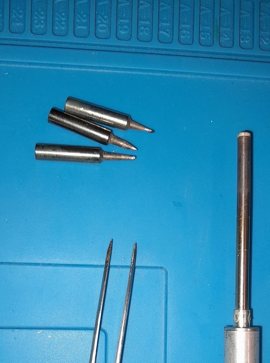
image

I have several, to use with an iron that I like. But I don't like soldering with the conical tips. I am not good at it.
That's going to change this year. I'm going to try and always use these tips when appropriate, and learn to love them.
The real goal is to become better at soldering with the conical versions than I am now with chisel and sloped types. And to enjoy the adaption path.

I'll keep you posted.

  • Sign in to reply
  • Cancel

Top Replies

  • shabaz
    shabaz over 2 years ago in reply to ntewinkel +5
    Hehe at least you got a choice : ) I didn't know of any other styles growing up, other than bevel. All the instructions taught everyone to use this style of tip: This is from the children's Ladybird…
  • shabaz
    shabaz over 2 years ago +4
    Maybe they are good on QFN. They look like they could be usable to drag the tip right into the corner when manually soldering QFN. I'm the same, no good with conical. Although the very finest/pointiest…
  • Gough Lui
    Gough Lui over 2 years ago +4
    I've used my conical so much that it's "turned" into a chisel :). My technique hasn't changed much really ... but I do prefer conical for the potential for fine-pitch touch-ups. Not as nice for transferring…
Parents
  • kmikemoo
    kmikemoo over 2 years ago

    I've been tempted by this thread to try a chisel tip.  Up to this point, I've only had conical.  My favorite one is the slightly offset tip (900M-T-IS).

    • Cancel
    • Vote Up +2 Vote Down
    • Sign in to reply
    • Cancel
  • Jan Cumps
    Jan Cumps over 2 years ago in reply to kmikemoo

    Seems that my post convinced more people to abandon conical than to learn it Sweat smile

    • Cancel
    • Vote Up +4 Vote Down
    • Sign in to reply
    • Cancel
  • shabaz
    shabaz over 2 years ago in reply to ntewinkel

    Perhaps, if it corrodes there. Or it could shock the entire board (although most components are a lot more rugged these days than they used to be).

    I don't know the chemical reasons for it, but I guess the exposed copper/plating/solder could interact all together with moisture and air.

    I doubt it matters at all with modern components being used indoors, but it's a habit (and does mean the joints visually look nicer with solder all over them!

    • Cancel
    • Vote Up +1 Vote Down
    • Sign in to reply
    • Cancel
  • shabaz
    shabaz over 2 years ago in reply to Jan Cumps

    It's seen a lot in videos from (say) Adafruit etc. Wrong though! (I mean if they are going to teach, they may as well try to do it properly, since it's little effort).

    • Cancel
    • Vote Up +2 Vote Down
    • Sign in to reply
    • Cancel
  • beacon_dave
    beacon_dave over 2 years ago in reply to shabaz

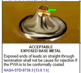
    Also depends if the cut is to be coated afterwards or not.

    image

    https://workmanship.nasa.gov/lib/insp/2%20books/frameset.html

    • Cancel
    • Vote Up +2 Vote Down
    • Sign in to reply
    • Cancel
  • shabaz
    shabaz over 2 years ago in reply to beacon_dave

    I think it is still cut first, i.e. this was a scenario where the soldering didn't cover the top of the joint despite it being cut beforehand. Not sure! 

    I guess this shows it must be a chemical reason, e.g. corrosion.

    • Cancel
    • Vote Up +2 Vote Down
    • Sign in to reply
    • Cancel
  • Jan Cumps
    Jan Cumps over 2 years ago in reply to shabaz

    I have an opinion®:

    the cut end of a lead is exactly the same material as all the rest of the lead. And that's exposed too.

    • Cancel
    • Vote Up +1 Vote Down
    • Sign in to reply
    • Cancel
  • beacon_dave
    beacon_dave over 2 years ago in reply to shabaz

    Yes, I was referring to the base metal sealing there.

    Strange that they let that one through though given some of the other stuff.

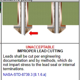
    I think this is the one you are after about cutting stress

    image

    • Cancel
    • Vote Up +1 Vote Down
    • Sign in to reply
    • Cancel
  • shabaz
    shabaz over 2 years ago in reply to beacon_dave

    I've not read the NASA standards, but it would be surprising if they allow component leads to be snipped on a PCB after the component is soldered. (merely from what I observed in mil-product hand assembly).  I know nothing about metallurgy/chemistry, so I'm speculating it is shock and corrosion related. But the conformal coating comment does seem to align with the corrosion theory (at the junction of the exposed copper/plating/solder perhaps, but I have no idea). 

    • Cancel
    • Vote Up +2 Vote Down
    • Sign in to reply
    • Cancel
  • hlipka
    hlipka over 2 years ago in reply to shabaz

    Here is what is done in avionics: https://www.youtube.com/watch?v=Vynb_HdEIDU . Whatever you do currently, it will not be good enough for these standards. (and yes, the cut before soldering)

    • Cancel
    • Vote Up +3 Vote Down
    • Sign in to reply
    • Cancel
  • shabaz
    shabaz over 2 years ago in reply to Jan Cumps

    You could be right, but instinctively if I see exposed copper on the end of a component, I tend to solder over it. Just habit.

    • Cancel
    • Vote Up +2 Vote Down
    • Sign in to reply
    • Cancel
  • beacon_dave
    beacon_dave over 2 years ago in reply to shabaz

    'Properly' kind of depends on which standards you are working to though.

    Also it doesn't help that some of those standards are expensive to get hold of and certification even more expensive...

    • Cancel
    • Vote Up +2 Vote Down
    • Sign in to reply
    • Cancel
Reply
  • beacon_dave
    beacon_dave over 2 years ago in reply to shabaz

    'Properly' kind of depends on which standards you are working to though.

    Also it doesn't help that some of those standards are expensive to get hold of and certification even more expensive...

    • Cancel
    • Vote Up +2 Vote Down
    • Sign in to reply
    • Cancel
Children
  • shabaz
    shabaz over 2 years ago in reply to beacon_dave

    We could rephase to "more properly " I guess : ) There are some things that seem to be common to all the standards, but some people take shortcuts like combing all the leads down like hair first, for all the components, and then soldering and then cropping. I think I saw it in an Adafruit or Sparkfun video. It might save half an hour on a project at most I guess.

    • Cancel
    • Vote Up +2 Vote Down
    • Sign in to reply
    • Cancel
  • dougw
    dougw over 2 years ago in reply to beacon_dave

    That is true. I run across NASA standards periodically and they provide some interesting insights, but are often different form other standards on the same topic. That said, I violate virtually every standard when I solder, and I'll even cut my own corners when some other requirement has higher priority. Like trimming the lead way too close to the card because there isn't enough room for a good solder joint. I do at least try to make the joint work for its intended application, and so far it is working out.

    • Cancel
    • Vote Up +2 Vote Down
    • Sign in to reply
    • Cancel
  • ntewinkel
    ntewinkel over 2 years ago in reply to beacon_dave
    beacon_dave said:
    'Properly' kind of depends on which standards you are working to though.

    That’s how I feel about it too. I imagine NASA would be the highest standard given the conditions the electronics for avionics and space flight would be used in: extreme vibration, temperature, and pressures. Maybe exposure to chemicals and gases too.

    Adafruit is geared towards hobby projects, so I imagine they’d rather not scare off the newbies with that level of precision! Similar for any beginner type classes.

    My standards will be slightly below that hobby level Rolling eyes

    I do want to start making them more visually appealing though, which includes cleaning of the flux and having more consistent solder joints.

    • Cancel
    • Vote Up +2 Vote Down
    • Sign in to reply
    • Cancel
  • dougw
    dougw over 2 years ago in reply to ntewinkel

    Leaving flux uncleaned - guilty as charged. Disappointed

    • Cancel
    • Vote Up +1 Vote Down
    • Sign in to reply
    • Cancel
  • dougw
    dougw over 2 years ago in reply to ntewinkel

    Maybe we should start a discussion  topic - How not to solder...Smiling imp

    • Cancel
    • Vote Up +3 Vote Down
    • Sign in to reply
    • Cancel
element14 Community

element14 is the first online community specifically for engineers. Connect with your peers and get expert answers to your questions.

  • Members
  • Learn
  • Technologies
  • Challenges & Projects
  • Products
  • Store
  • About Us
  • Feedback & Support
  • FAQs
  • Terms of Use
  • Privacy Policy
  • Legal and Copyright Notices
  • Sitemap
  • Cookies

An Avnet Company © 2025 Premier Farnell Limited. All Rights Reserved.

Premier Farnell Ltd, registered in England and Wales (no 00876412), registered office: Farnell House, Forge Lane, Leeds LS12 2NE.

ICP 备案号 10220084.

Follow element14

  • X
  • Facebook
  • linkedin
  • YouTube