Silicon Carbide Diodes and MOSFETs have become the favored device for high-voltage power-converter applications. These devices have breakdown voltages as high as 1700 V while featuring Rds-On in the 10s of milliohms and can be switched up to 400 kilohertz. In this video, learn what makes silicon carbide transistors different, the applications where they work best, and and how you can simulate converter designs using onsemi's unique tools.
Watch the Video:
Introduction to SiC
Traditional silicon transistors are incredibly versatile devices that have been around for almost 70 years! About 20 years ago, a new type of MOSFET hit the market. Instead of Silicon, it featured a Silicon Carbide (SiC) substrate. This new wideband gap material offers significant advantages over traditional MOSFETs, especially in high-voltage (>650 V) applications like power converters for solar, UPS, and Electric Vehicles (EV).
![]()
At its core, Silicon Carbide is a hard chemical substance made of Silicon and Carbon. It is a semiconductor material and is known for its wide bandgap properties. As a semiconductor, it has obvious uses as transistors and didoes.
Applications for SiC Devices
Today, you will find Silicon Carbide diodes and transistors in applications like utility-grade solar panel inverters, industrial energy storage (uninterrupted power supplies), and electrical vehicle (EV) chargers. For EVs, SiC is in both onboard chargers and external charging stations.

In the past, these converters used IGBTs. However, those devices are limited to switching speeds of about 50 kilohertz. For comparison, traditional power MOSFETs run up to about 100 kilohertz, and SiC MOSFETs can run up to 400 kilohertz! These increased switching speeds are significant because they reduce the size of the design's capacitors and inductors, reducing overall cost.
Difference between Si and SiC MOSFET

If you compare the layers found in a Silicon (Si) or Silicon Carbide (SiC) MOSFET, you can see the same elements! The material difference is only the substrate itself. The rest of the doped layers are practically the same.
However, a pivotal difference to recognize is that the N- Drift Layer is thinner in SiC devices than in Si devices. And that difference is because of SiC’s wide bandgap properties.

The much higher dielectric breakdown field strength makes the Silicon carbide’s drift layer thinner than a traditional Silicon MOSFET while providing a higher breakdown voltage! In other words, a 600V SiC MOSFET is much thinner than a 600V Si MOSFET. And related, 1700 volt SiC devices are still relatively thin.
Another reason this thickness (or thinness!) is important is that it dominates the device’s on-resistance (between drain and source.) So when the MOSFET is off, it can tolerate very high voltages, and when it is on, it dissipates very little heat.
The higher electron saturation velocity also enables a SiC MOSFET to switch on and off faster, giving SiC MOSFETs a higher operating frequency.

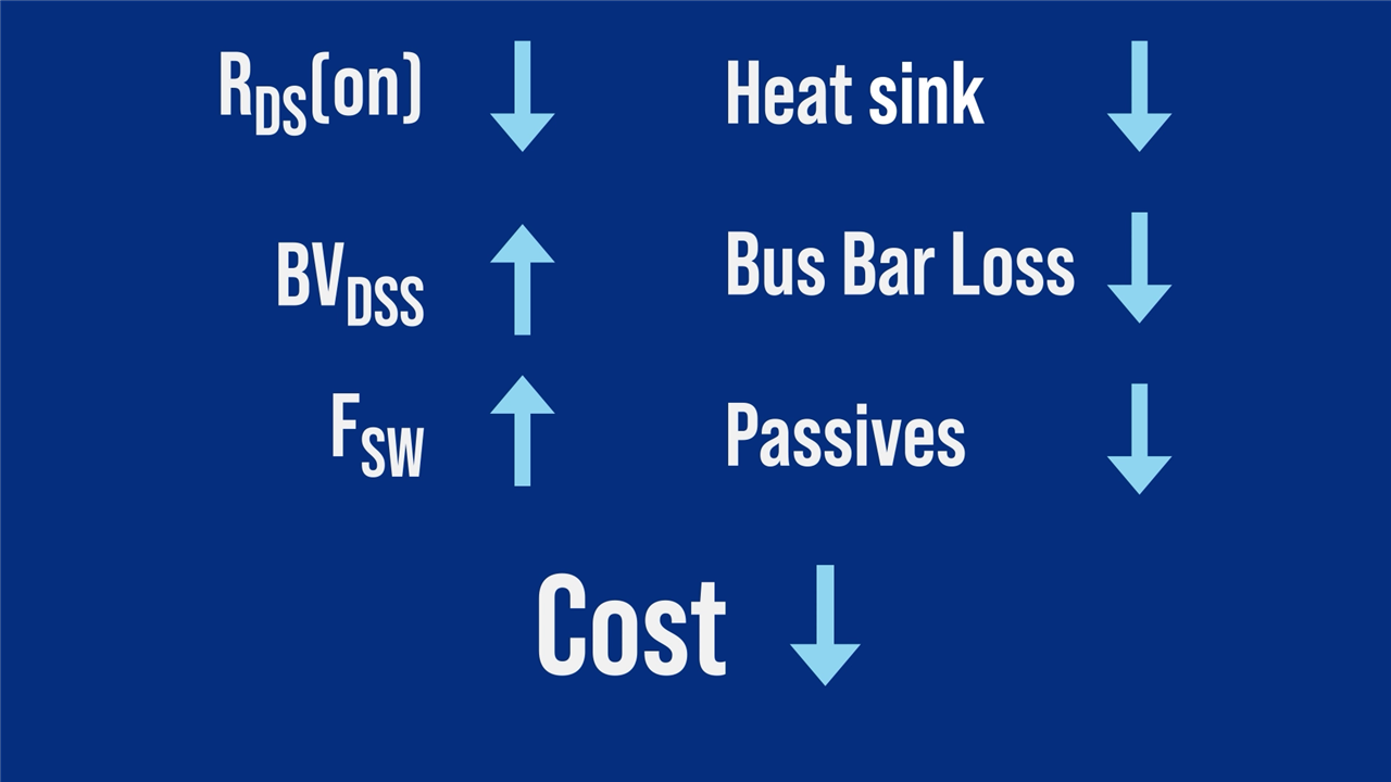
These advantages add to a lower cost-cost design for power converters in the kilowatt and megawatt range. The lower on-resistance means less heat sinks, the higher breakdown voltage means smaller bus bars and the higher switching frequency means small passives. All of these factors contribute to the lower overall cost of a design.
Simulating SiC
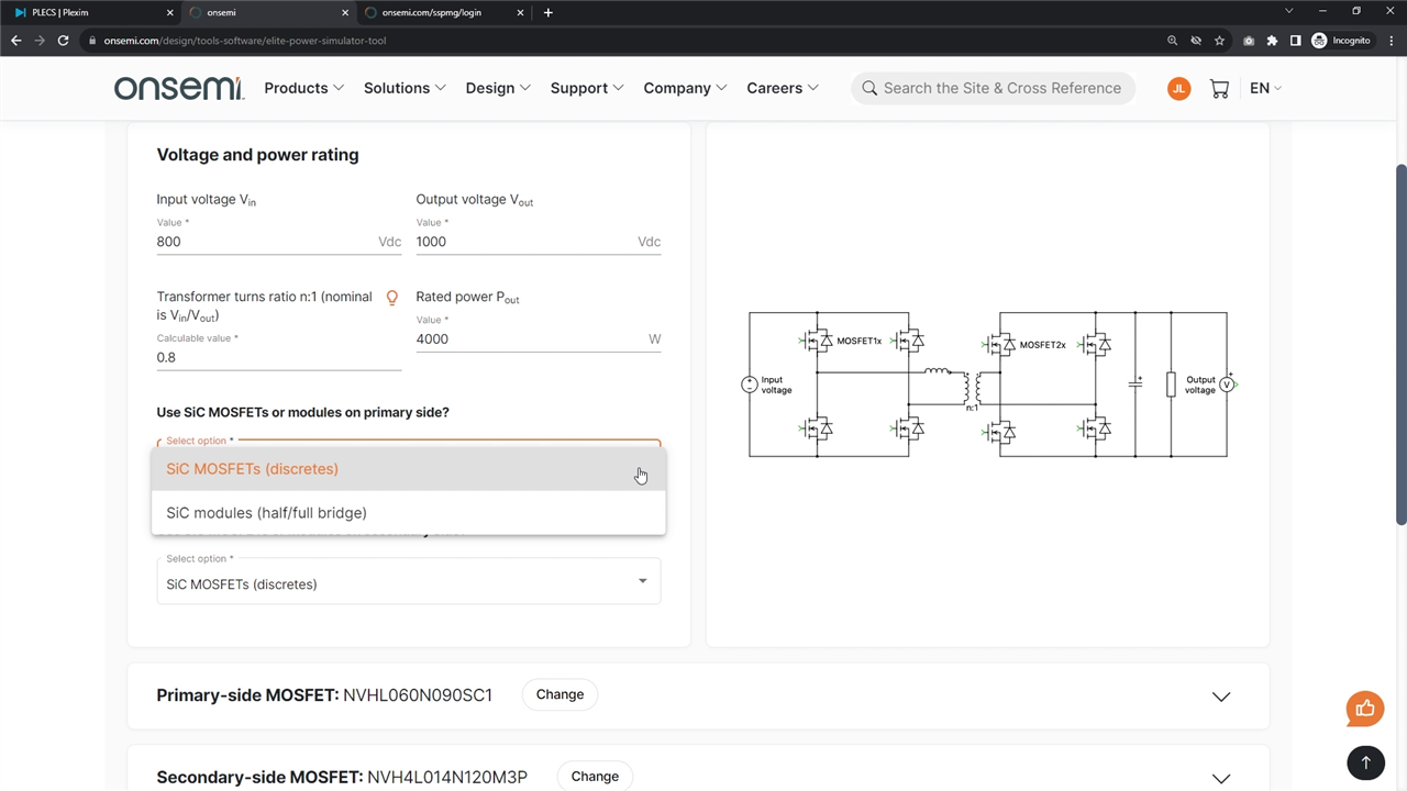
onsemi offers the Elite Power Simulator so you can simulate power converters with EliteSic Silicon Carbide transistors. The backend tool is based on the industry-standard PLECS simulator from Plexim.

Elite Power Simulator’s step-by-step approach makes it easy to change topologies, voltages, switching frequencies, and devices used in the design. One unique advantage that onsemi offers, though, is customized loss models.
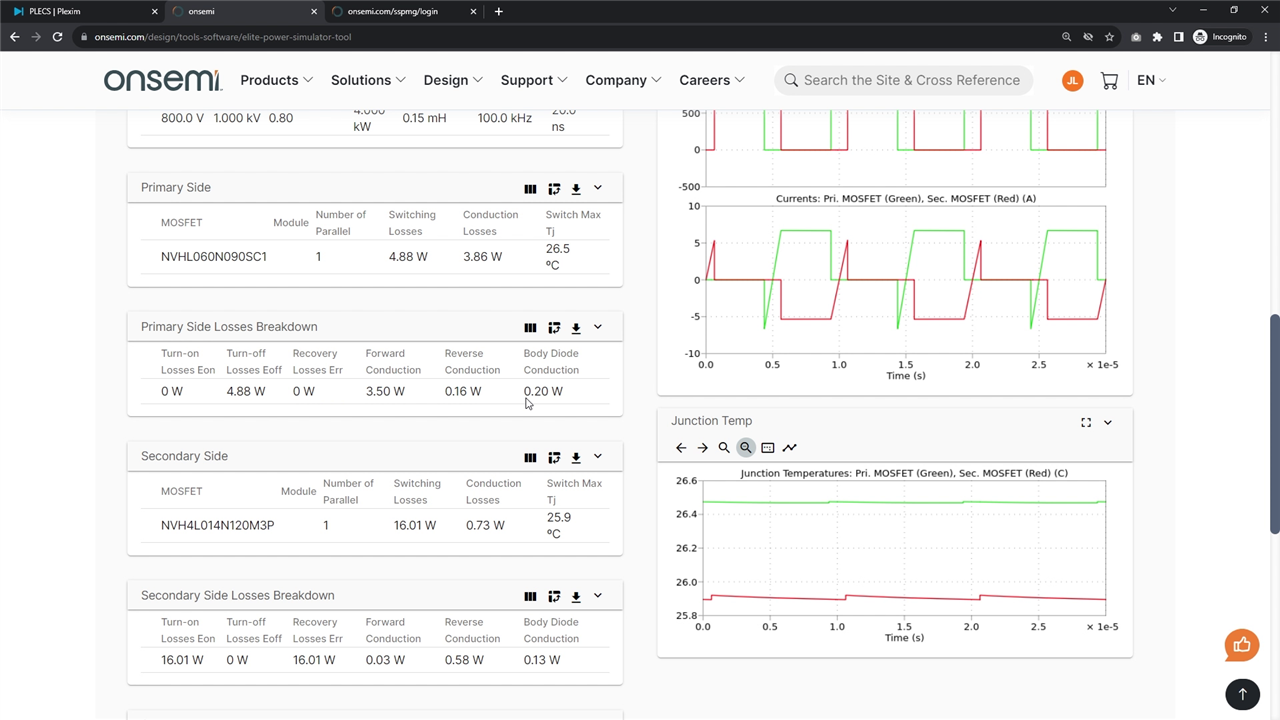
One of the most critical pieces of data you can get from a power electronics simulation is the switching losses of the semiconductors. And while most vendors offer models for their devices, they are built on a limited dataset.

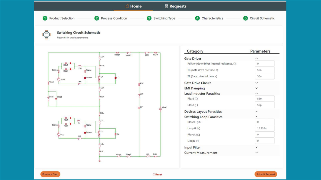
onsemi’s Self-Service PLECS Model Generator tool creates application-specific models for you. The tool starts with the physical characteristics of the EliteSiC device. Then it combines that with parameters from your test or design setup.

The parameters you can add are highly detailed but result in far more accurate models. The generator does take a little bit of time to generate them. However, the process is entirely automated. In other words, you do not have to wait for an Application Engineer to get back to you! Once you download the models, you can use them in the Elite Power Simulator and get detailed results from the simulator.

Check out the links below to these onsemi tools and to learn more about their range of Silicon Carbide devices:

Top Comments