


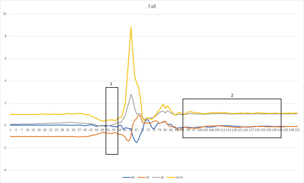
As I said in this blog, I experienced a lot issues when I tried to run the neural network on the Arduino Nano 33 IoT and I switched to a classic threshold-based algorithm to detect a fall. In a few words, I will detect three phases of the fall
- free-fall (rectangle "1" in picture below)
- impact
- inactivity (rectangle "2" in picture below)
Currently, all these operations are performed by the SAM21D MCU, but the LSM6DS3 IMU includes a lot of interesting features that worth to be investigated to off-load some of the computations from the SAMD21D MCU to the LSM6DS3 IMU.
The idea is to extend the LSM6DS3 library by adding proper methods to configure free-fall, impact and inactivity detection parameters
The original LSM6DS3 library
The original LSM6DS3 implements three functions that are going to be very useful for my work
class LSM6DS3Class {
  public:
[...]

  private:
    int readRegister(uint8_t address);
    int readRegisters(uint8_t address, uint8_t* data, size_t length);
    int writeRegister(uint8_t address, uint8_t value);

[...]


};
These three functions will give me full access to any register in the IMU chip, so I can configure detection algorithms according to my needs
Initialization
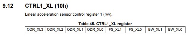
The LMS6DS3 must be initialized. This task is already accomplished by the original library, which writes register CTRL1_XL
This is how the Arduino library initializes the LMS6DS3
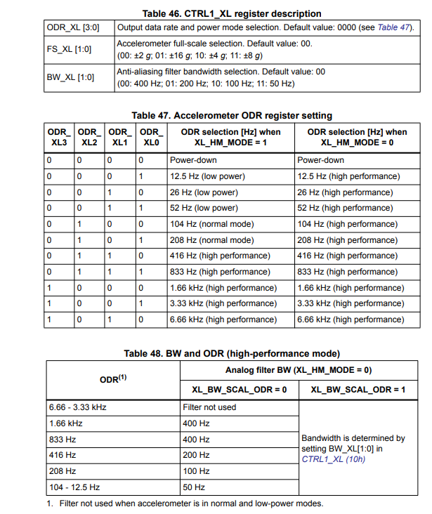
  //set the gyroscope control register to work at 104 Hz, 2000 dps and in bypass mode
  writeRegister(LSM6DS3_CTRL2_G, 0x4C);


  // Set the Accelerometer control register to work at 104 Hz, 4G,and in bypass mode and enable ODR/4
  // low pass filter(check figure9 of LSM6DS3's datasheet)
  writeRegister(LSM6DS3_CTRL1_XL, 0x4A);


  // set gyroscope power mode to high performance and bandwidth to 16 MHz
  writeRegister(LSM6DS3_CTRL7_G, 0x00);


  // Set the ODR config register to ODR/4
  writeRegister(LSM6DS3_CTRL8_XL, 0x09);
The important thing here is the ODR_XL (Accelerometer Output data rate), which is set to 104 Hz (4Ah is written in CTRL1_XL register) and is required when we will have to calculate to values to write into configuration registers
ODR_XL=104 Hz
FS_XL = 4g
Free-fall detection
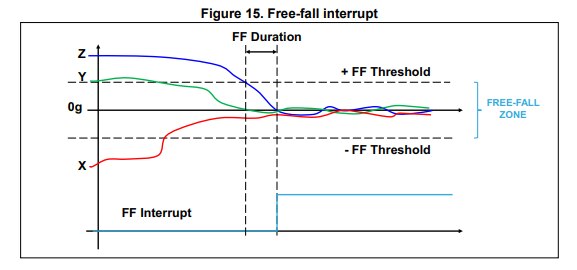
Free-fall detection refers to a specific register configuration that allows recognizing when the device is in free-fall: the acceleration measured along all the axes goes to zero. In a real case a “free-fall zone” is defined around the zero-g level where all the accelerations are small enough to generate the interrupt. Configurable threshold and duration parameters are associated to free-fall event detection: the threshold parameter defines the free-fall zone amplitude; the duration parameter defines the minimum duration of the free-fall interrupt event to be recognized
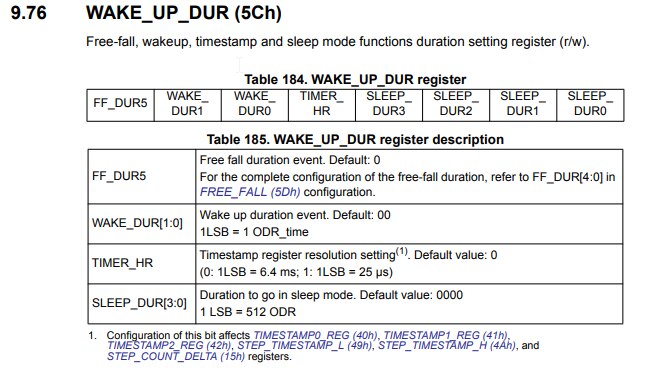
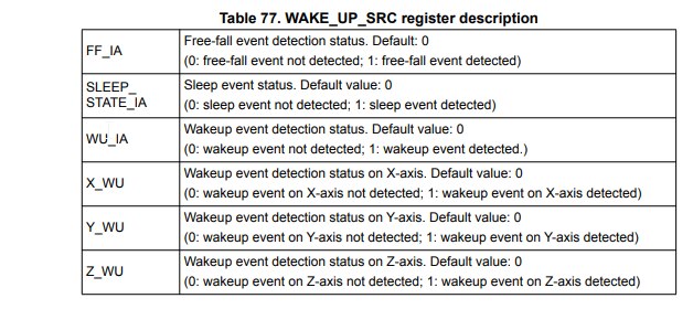
Free-fall threshold duration and threshold are set in register FREE_FALL and WAKE_UP_DUR, whose content is shown in screenshot below (from LSM6DS3 datasheet)
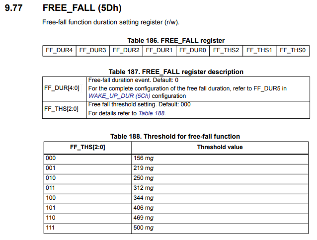
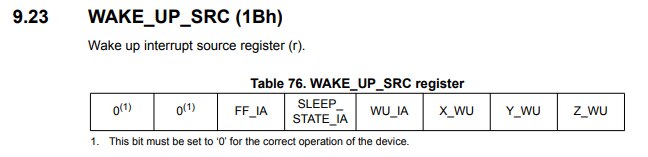
The free-fall condition can be checked by reading the FF_IA bit of the WAKE_UP_SRC register. However, there are some caveats here. By default, the free-fall condition is not latched (LIR bit of the TAP_CFG register)
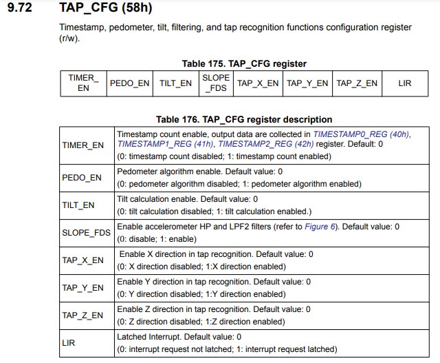
This means that the FF_IA bit is set when the free-fall condition is detected and reset when the free-fall condition is no longer there. This may lead to loose events, because we poll the IMU at a fixed rate, and the event may occur between two polls. For sure, we need to enable latch mode. But if the latch mode is enabled but the interrupt signal is not driven to the interrupt pins, the latch feature does not take effect. This means we need to drive the free-fall interrupt signal to a pin, even if the pin on the Arduino Nano 33 IoT is not connected. The free-fall interrupt signal can be driven to the two interrupt pins by setting to 1 the INT1_FF bit of the MD1_CFG register or the INT2_FF bit of the MD2_CFG register. With these settings, latch mode can be enabled and, when a free-fall event has occurred and the interrupt pin is asserted, it must be reset by reading the WAKE_UP_SRC register.
Pseudo-code
To summarize, here is the pseudo-code required to initialize free-fall detection
- Set event duration (FF_DUR5 bit) - Write 00h into WAKE_UP_DUR
- Set FF threshold (FF_THS[2:0] = 011b) and set six samples event duration (FF_DUR[5:0] = 000110b) - Write 33h into FREE_FALL
- Drive free-fall interrupt to INT1 pin - Write 10h into MD1_CFG
- Latch interrupt - Write 01h into TAP_CFG
To check if a free-fall event has occurred, read register WAKE_UP_SRC and check if bit 5 (FF_IA) is set
Impact detection
The LSM6DS3 device can be configured to output an interrupt signal when tapped (once or twice) in any direction: the TAP_X_EN, TAP_Y_EN and TAP_Z_EN bits of the TAP_CFG register must be set to 1 to enable the tap recognition on X, Y, Z directions, respectively.
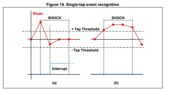
Configurable parameters for tap recognition functionality are the tap threshold and the Shock, Quiet and Duration time windows.
The TAP_THS[4:0] bits of the TAP_THS_6D register are used to select the unsigned threshold value used to detect the tap event. The value of 1 LSB of these 5 bits depends on the selected accelerometer full scale: 1 LSB = (FS_XL)/(25). The unsigned threshold is applied to both positive and negative slope data. The Shock time window defines the maximum duration of the overthreshold event: the acceleration must return below the threshold before the Shock window has expired, otherwise the tap event is not detected. The SHOCK[1:0] bits of the INT_DUR2 register are used to set the Shock time window value: the default value of these bits is 00b and corresponds to 4/ODR_XL time, where ODR_XL is the accelerometer output data rate. If the SHOCK[1:0] bits are set to a different value, 1 LSB corresponds to 8/ODR_XL time.
In the double-tap case, the Quiet time window defines the time after the first tap recognition in which there must not be any overthreshold. When the latch mode is disabled (LIR bit of TAP_CFG is set to 0), the Quiet time also defines the length of the interrupt pulse (in both single and double-tap case). The QUIET[1:0] bits of the INT_DUR2 register are used to set the Quiet time window value: the default value of these bits is 00b and corresponds to 2/ODR_XL time, where ODR_XL is the accelerometer output data rate. If the QUIET[1:0] bits are set to a different value, 1 LSB corresponds to 4/ODR_XL time.
Tap interrupt signals can also be checked by reading the TAP_SRC (1Ch) register
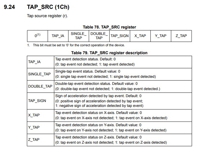
- TAP_IA is set high when a single-tap or double-tap event has been detected.
- SINGLE_TAP is set high when a single tap has been detected.
- DOUBLE_TAP is set high when a double tap has been detected.
- TAP_SIGN indicates the acceleration sign when the tap event is detected. It is set low in case of positive sign and it is set high in case of negative sign.
- X_TAP (Y_TAP, Z_TAP) is set high when the tap event has been detected on the X (Y, Z) axis.
Single and double-tap recognition works independently. To enable only the single-tap recognition. we need to set the SINGLE_DOUBLE_TAP bit of WAKE_UP_THS to 0.
If the latch mode is enabled and the interrupt signal is driven to the interrupt pins, the value assigned to SINGLE_DOUBLE_TAP also affects the behavior of the interrupt signal: when it is set to 0, the latch mode is applied to the single-tap interrupt signal; when it is set to 1, the latch mode is applied to the double-tap interrupt signal only. The latched interrupt signal is kept high until the TAP_SRC register is read. If the latch mode is enabled but the interrupt signal is not driven to the interrupt pins, the latch feature does not take effect.
Pseudo-code
Here is the pseudo-code to configure impact detection
- Enable tap detection on X, Y, Z axis - Write 0Eh into TAP_CFG
- Set tap threshold - Write 0Bh into TAP_THS_6D
- Set Quiet and Shock time windows - Write 00h into INT_DUR2
- Only single tap enabled (SINGLE_DOUBLE_TAP = 0) - Write 00h into WAKE_UP_THS
- Single tap interrupt driven to INT1 pin - Write 40h into MD1_CFG
- Latch interrupt - Write 01h into TAP_CFG
The TAP_THS field of the TAP_THS_6D register is set to 01011b, therefore the tap threshold is 1375 mg (= 11 * FS_XL / 2^5).
The SHOCK field of the INT_DUR2 register is set to 10b: an interrupt is generated when the slope data exceeds the programmed threshold, and returns below it within 19.8 ms (= 2 / ODR_XL) corresponding to the Shock time window.
Activity/inactivity recognition
The Activity/Inactivity recognition function was actually designed to reduce system power consumption, but in this case we will use this feature to determine if the elder is motionless or not.
When the Activity/Inactivity recognition function is activated, the LSM6DS3 device is able to automatically decrease the accelerometer sampling rate to 12.5 Hz, increasing the accelerometer ODR and bandwidth as soon as the wake-up interrupt event has been detected. This feature is applied to the accelerometer sensor only, regardless of the selected gyroscope power mode and ODR. The maximum allowed accelerometer ODR (configurable through the ODR_XL [3:0] bits of the CTRL1_XL register) for using the Activity/Inactivity feature is 833 Hz.
With this feature the system may be efficiently switched from low-power consumption to full performance and vice-versa depending on user-selectable acceleration events, thus ensuring power saving and flexibility.
The Activity/Inactivity recognition function is enabled by setting to 1 the INACTIVITY bit of the WAKE_UP_THS register.
In the LSM6DS3 device the Activity/Inactivity recognition function can be implemented using either the slope filter or the high-pass digital filter.
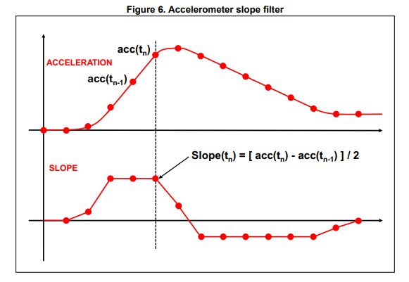
The filter to be applied can be selected using the SLOPE_FDS bit of the TAP_CFG register: if this bit is set to 0 (default value), the slope filter is used; if it’s set to 1, the high-pass digital filter is used.
This function can be fully programmed by the user in terms of expected amplitude and timing of the slope data by means of a dedicated set of registers.
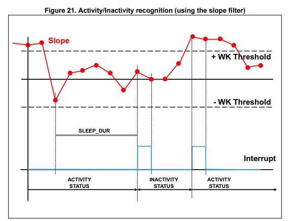
The unsigned threshold value is defined using the WK_THS[5:0] bits of dedicated set of registers WAKE_UP_THS register
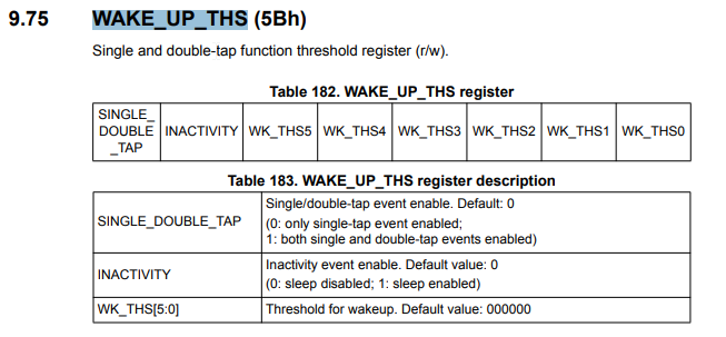
The value of 1 LSB of these 6 bits depends on the selected accelerometer full scale: 1 LSB = (FS_XL)/(2^6). The threshold is applied to both positive and negative filtered data.
When a certain number of consecutive X,Y,Z slope data is smaller than the configured threshold, the ODR_XL [3:0] bits of the CTRL1_XL register are bypassed (Inactivity) and the accelerometer is internally set to 12.5 Hz although the content of CTRL1_XL is left untouched. The duration of the Inactivity status to be recognized is defined by the SLEEP_DUR[3:0] bits of the WAKE_UP_DUR register: 1 LSB corresponds to 512/ODR_XL time, where ODR_XL is the accelerometer output data rate.
Once the Activity/Inactivity detection function is enabled, the status can be driven to the two interrupt pins by setting to 1 the INT1_INACT_STATE bit of the MD1_CFG register or the INT1_INACT_STATE bit of the MD2_CFG register; it can also be checked by reading the SLEEP_STATE_IA bit of the WAKE_UP_SRC register.
Pseudo-code
Here is the pseudo-code to initialize the activity detection
- Set duration for Inactivity detection - Write 01h into WAKE_UP_DUR
- Set Activity/Inactivity threshold, Enable Activity/Inactivity detection - Write 42h into WAKE_UP_THS
- Activity/Inactivity interrupt driven to INT1 pin - Write 80h into MD1_CFG
In this example the WK_THS field of the WAKE_UP_THS register is set to 000010b, therefore the Activity/Inactivity threshold is 125 mg (= 2 * FS_XL / 2^6).
Before Inactivity detection, the X,Y,Z slope data must be smaller than the configured threshold for a period of time defined by the SLEEP_DUR field of the WAKE_UP_DUR register: this field is set to 0010b, corresponding to 4.92 s (= 1 * 512 / ODR_XL). After this period of time has elapsed, the accelerometer ODR is internally set to 12.5 Hz.
The Activity status is detected and the CTRL1_XL register settings immediately restored if the slope data of (at least) one axis are bigger than the threshold.
| Previous post | Source code | Next post |
|---|---|---|
| ACE - Blog #7 - Improving the device construction | https://github.com/ambrogio-galbusera/ace2.git | ACE - Blog #9 - Conclusions |
Top Comments