This is my fourth blog post in a series that cover my experience going through the training courses of the Path to Programmable 3 challenge. The first three blog posts, Blog1, Blog2, and Blog3, have covered the beginning of participating in this challenge and my learning experience from going through the SW Lab 0 to Lab 11. Now I am continuing with the HW labs.
The hardware labs consist of 9 labs plus lab 0 which is primarily setting up the training files and the Vivado tools environment. First experiment was to setup the virtual machine. This is similar to Experiment 1 in the software training sequence. So I came to the same conclusion like I did for the software training Lab 0, which has guided me to installing an Ubuntu Linux virtual machine on a Windows computer. I didn’t fully understand the reason for installing the virtual machine but what I get is that the PetaLinux tools work only on certain versions of Ubuntu, and this virtual machine would create a mode of operation for the Windows computer that would function like the Ubuntu 18.04 version. Based on the lab instructions I have figured out that the process of installing this virtual machine is very complicated and with some risk as I would have to make some changes in the computer bios system.
And the big problem that I saw for myself, is that if the virtual machine messes up my computer there are no instructions on how to uninstall it. The un-installation I assume is quite complicated too since the memory allocation in the hard drive has to be un-done and the changes in the computer bios have to be undone.
So I took the decision to use a separate computer for the PetaLinux part of the training and design challenge, which I will setup up with a separate hard drive and on which I will install directly Ubuntu version 18.04.
The second experiment of Lab 0, to setup the training lab files, went smoothly by just following the step-by-step instructions, so I got to the next lab, Lab 1.
Lab 1 was also easy, as I only had to setup a new project in Vivado. I already knew how to do this from my past experience working with FPGAs, so I went fast through these steps. The lab instructions are well written for this part, and they covered how to create a new project, how to setup the FPGA part number, how to create a block design using the IP integrator design flow, and how to add an embedded ARM processor to the project.
This was a long lab with intense instructions. I had to concentrate a lot to make sure I don’t miss any detail. On experiment 4 I have created a “Hello World” application following the provided instructions. This was interesting; however, I would have preferred to actually write the code myself since anyway it was just a simple C code. The lab setup has just provided too much for us so we only had to do “click”. “click”. … until we got to see the results.
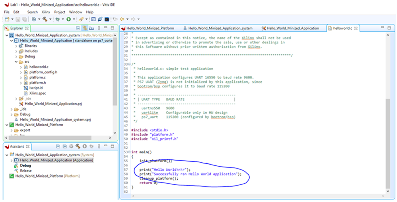
This was just a simple code that probably any course participant would have been able to write. Building the project and programming the Zynq SoC FPGA happened without any issue. Then I have run the application and the Lab instructions asked me to use the GTKterm in the Ubuntu virtual machine. However, I didn’t have the virtual machine installed together with my Windows system for the reasons that I have mentioned above.

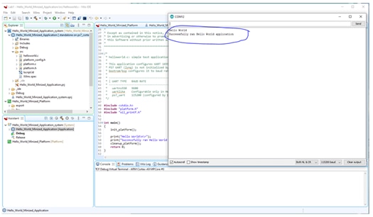
So having Ubuntu on a different machine didn’t help here since the USB cable was connected to the Windows computer. Thus, I had to find another solution for monitoring the COM serial port. Luckily, I remembered that I had the Arduino environment installed on the same Windows machine and that tool has a serial port monitor function. This method worked well, and I was able to read back the message from the Zynq application on the Arduino serial monitor panel:
Next I’ve got into more interesting stuff as I started Lab 3. The first experiment has thought me how to map the PS peripherals, which in our case has to match the connections on the MiniZed evaluation board. In other cases it has to match the connection on the corresponding board. The lab instructions points us to create a new folder for Lab3 and copy the files from the solutions folder. I personally would have preferred to start from scratch with a “blank” project, but in this case I have just followed the instructions. In the copied project there is the ZYNQ7 Processing System that I have customized based on the lab instructions. The customization included the Quad SPI Flash, USB 0 peripheral, SD card, GPIO, and UART 1:
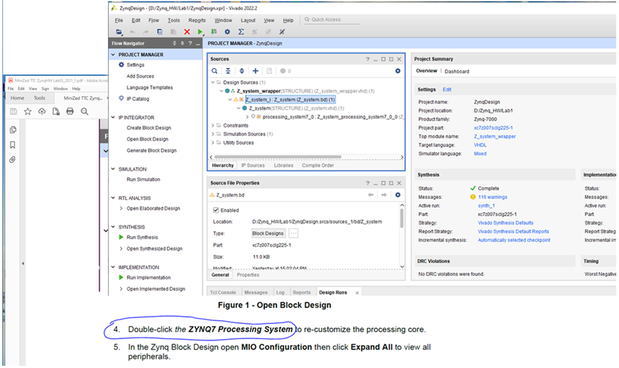
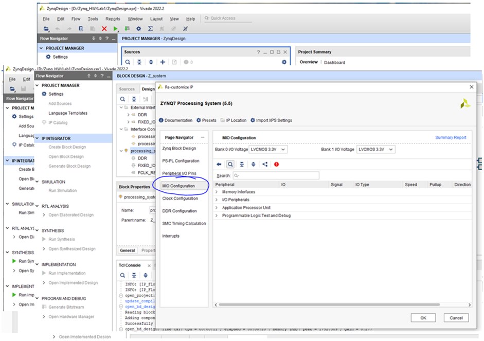
Then I double clicked on this block:
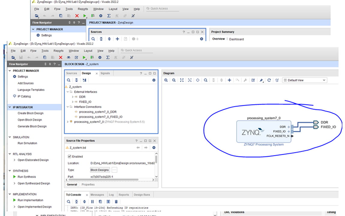
and customize the MIO configuration:
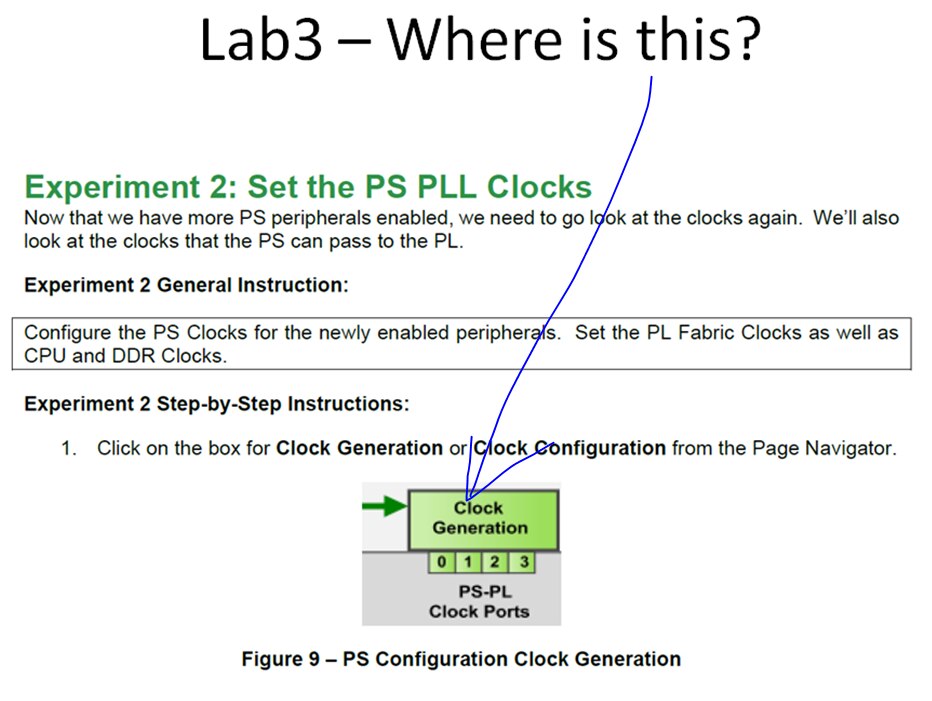
Next experiment has thought me how to set the PS PLL clocks. Here I’ve got a bit confused with the instructions since they used a small screenshot of the ”Clock Generation” block but I just didn’t figure out immediately where to find that “Clock generation” block.
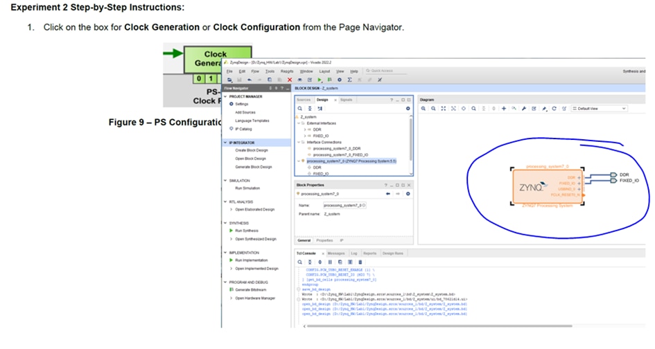
After a bit of “poking around” I have located it in the block diagram. It would have been easier if the instructions would have shown the entire block diagram with highlighted location of the clock generation block. Maybe it was only me who had trouble finding that block, but I had to double click on the PS block:
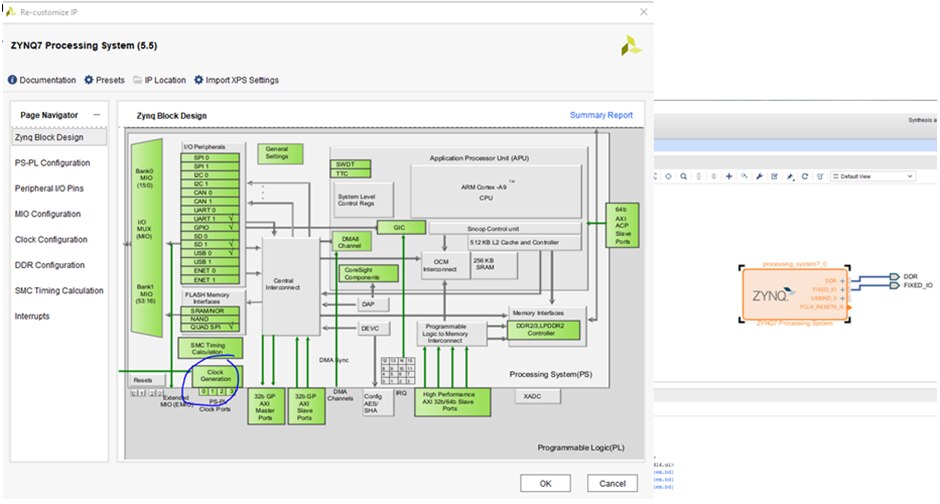
Which has then opened the block diagram that contained the clock generation block:
Setting up the clocks worked well just by following the instructions. Next step was to create and run test applications. The first application, “Hello World” didn’t work for me from just following the instructions:
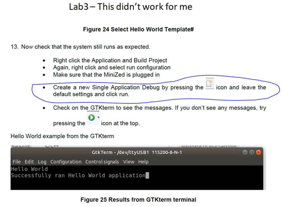
Luckily I have figured out a way to make it run, as I am showing in the figure below:
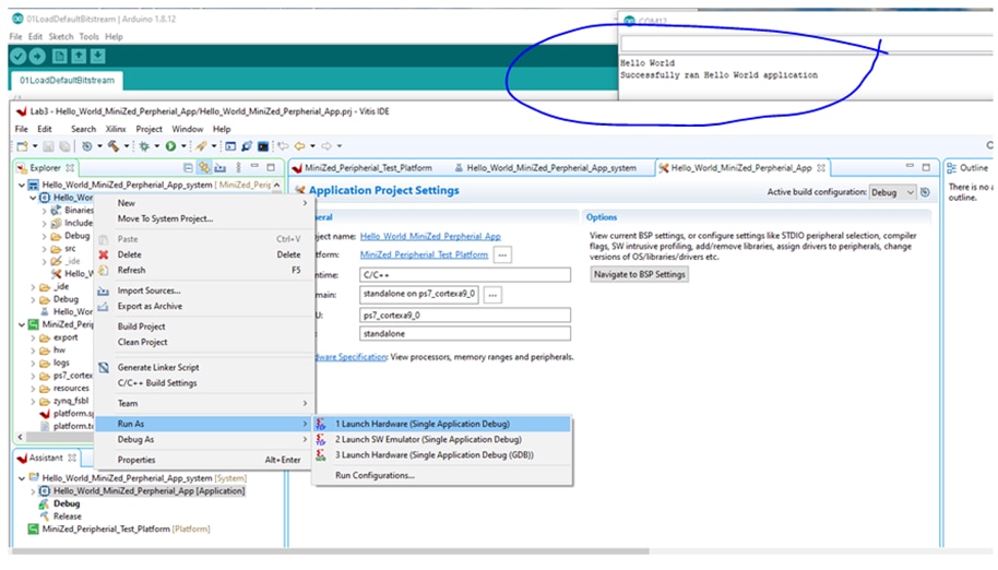
Since these applications are created in Vitis (as we have learned in the SW training labs) I had to export the project hardware to Vitis by clicking File then Export and then Export Hardware. He exported hardware has included also the bitstream file for programming the PL of the FPGA. I have then closed Vivado and opened Vitis. Once in VItis, I had to create first a platform project using the knowledge from the SW training labs. The hardware information exported from Vivado came in a single file with the .xsa extension. This lab instructions have repeated step-by-step the procedure, which actually was identical to the procedure that we learned in the SW training labs. On this platform project I have created then a application project for testing the memory “MiniZed_Memory_Test” and another application to test the peripherals. Next I programmed the MiniZed board and then run the two applications:

And the peripheral test:

However, occasionally I have received this error, and I had to cycle the power to fix it:
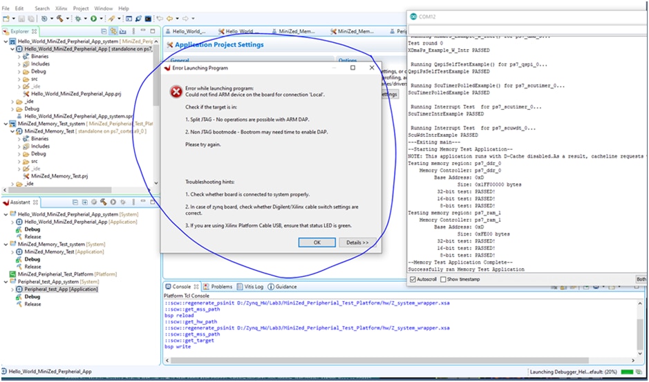
The error might be related with this note that I found in the instructions:

This concludes my experience working on HW Labs 1 - 3 and the third blog post in this series. I will come back with additional blog posts as I advance more through the Path to Programmable 3 tutorials.
Until then, all best wishes to the readers and the rest of participants.
Cosmin
