Blog # 1 - Project Description And Upgrade Installation
Blog # 2 - MiniZed Board Peripheral Configuration and Creating a Boot Image
Blog # 3 - Executing Vivado Design Suite TCL Commands
Blog # 4 - Move Data Between BRAM and DDR3 Memories
Blog # 5 - How to Enable Interrupts With MiniZed
**********************************************************************************************************************
In this tutorial I am going to show you how to move data from BRAM memory to DDR3 efficiently. Here I will use as a reference Lessons 5 and 6 of the training course. As an experiment I will change some of these data to verify performance. MiniZed Hardware Technical Training 2021.1: Lesson 5 and MiniZed Hardware Technical Training 2021.1: Lesson 6

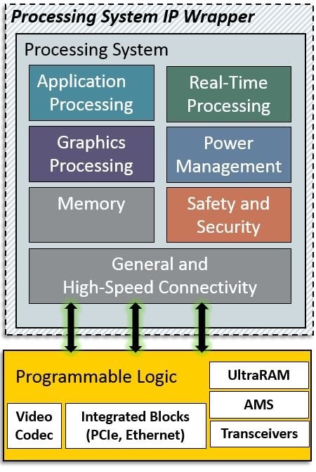
The Zynq UltraScale MPSoC family consists of a system-on-chip (SoC) style integrated processing system (PS) and a Programmable Logic (PL) unit, providing an extensible and flexible SoC solution on a single die.
Vivado
In Lesson 5, we used vivado to Add a BRAM from the IP Catalog, and Connect AXI peripherals to the Zynq PS. First we add AXI BRAM Controller.
The AXI BRAM Controller is a soft AMD IP core for use with the Embedded Development Kit (EDK) and Vivado IP Integrator (IPI).
I made double Click the AXI BRAM and Increase the Data Width to 64 bits, and change the Support for AXI Narrow Bursts to Manual. Also I ran connection automation. Then I check the box for All Automation.
The assistant has automatically added and connected a Block Memory Generator IP block.
The BRAM Controller expects to be a Slave on an AXI Interconnect. However, we will first need to configure a Master. Also we will need a clock accessible to that logic. So we made double-click the Zynq PS block. Then click on 32b GP AXI Master Ports.
Then, we check the box to select M AXI GP0 Interface.
Open clock configuration and enable fabric clock 0 by checking the box next to FCLK_CLK0, and set it to 50MHz.
Click OK to Zynq7 Processing System. After click Run Connection Automation we get the Block Design with AXI BRAM Controller and AXI Interconnect Connections as shown below.
On the AXI SmartConnect we can see the number of Master interfaces. If I want to add more slave IP, then I can increase this value here.
If we make click on window - address editor, we can check the 8K of memory located at 0x4000_0000.
After all this steps, we validate design, save the block design, reset output products, and generate output products, we can type this TCL command to improve the timing: set_property CONFIG.PCW_FCLK_CLK0_BUF TRUE [get_bd_cells /processing_system7_0]
After that, select Generate Bitstream from the Flow Navigator.
Vitis
After create a workspace, export hardware, and launch Vitis IDE, we create a platform project of name: BRAM_PLATFORM
Once Vitis has finished loading build the Platform.
Next, I import the previously created applications from Lab 3, just select File - Import. We will copy the apps from the lab3 software folder into the lab6 software folder. Select Eclipse workspace or zip file.
Now, I Browse to the ZynqDesign_lab3 directory, and the three applications are checked: Hello_World, Memory_Test and the Peripheral Test apps into our current project.
Also I verified the IP versions were loaded for the BRAM.
Now I create a new application project named BRAM_DMA_TEST
For this template we are going to use the Empty Application (C).
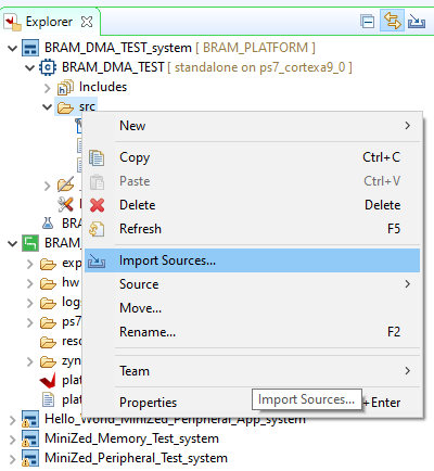
Now right-click on src and choose Import sources.

From the support documents we select "dma_test.c" file.
After Vitis build the project, we make right click the system app again and select Run As and select Launch Hardware. Below you can see a test.
Experiment
I changed the number of words in field 1 from 256 to 384 to verify if there was any change in the data,
   	   	switch(num_in)
    			{
    				case '1' :
    					//num = 256;
    					//print("Sending 256 bytes\r\n");
    					num = 384;
    					print("Sending 384 bytes\r\n");
    					break;
    				case '2' :
    					num = 512;
    					print("Sending 512 bytes\r\n");
    					break;
    				case '3' :
    					num = 1024;
    					print("Sending 1024 bytes\r\n");
    					break;
    				case '4' :
    					num = 2048;
    					print("Sending 2048 bytes\r\n");
    				    break;
    				case '5' :
    					num = 4096;
    					print("Sending 4096 bytes\r\n");
    					break;
    				case '6' :
    					num = 8192;
    					print("Sending 8192 bytes\r\n");
    					break;
    				default :
    					num = 256;
    					print("Sending 256 bytes\r\n");
    					break;
    			}
I show you the result below.
As we can see, the result was consistent, since the improvement was 13x for both cases. On the other hand moving data through DMA in interrupt mode took 2262 clock cycles in the first case (256) and 3381 in the second case (384).

