In this week; I also completed Lab 3, Lab 4 and Lab 5. The objectives of these labs were also very well written and rather simple to follow. These labs are a continuation from previous labs which can be found here
Lab 3
Main Objectives of this blog
• Enable and map all default peripherals in IP Integrator
• Set the PS clocks for the PS peripherals and the PL
• Create and Run C programs
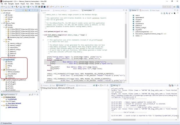
- Peripheral Tests
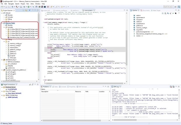
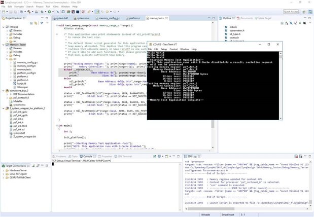
- Memory Test
Exp 1: Enable and map all default peripherals in IP Integrator.
The peripherals were modified in the MIO configuration window. The MIO config can be done by re-customizing the ZYNQ7 processing system. The peripherals such as Quad SPI Flash, USB0, SD card/eMMC should be enabled.
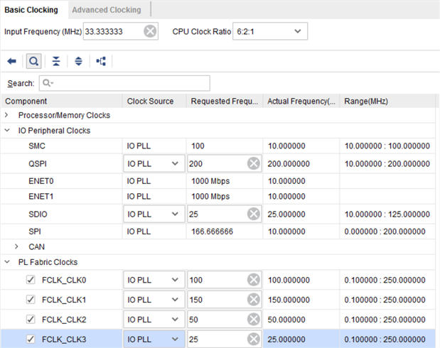
Exp 2: Set the PS clocks for the PS peripherals and the PL
Here we checked out how the PS Clock Wizard works and the different clock settings for the IO Peripheral Clocks; PL Fabric Clocks and the Processor/Memory Clocks. Each IO peripheral such as QSPI, SDIO, Ethernet needs its own clock frequency and this this can be changed in this wizard. The Zynq PS has three PLLs – ARM, DDR, and I/O
Now in the previous labs; we added the different peripherals and here we run peripheral tests on this hardware. These peripherals QSPI, SDIO, Ethernet are compiled in hardware from the previous lab 4 and lab 5. Now this hardware is exported from Vivado into SDK and tested by creating new Xilinx C/C++ Application on top of the bsp (Board support package).
Memory testing of the MInized board
Peripherals testing of the MInized board
Looking deeply into the power usage and connections established in the Minized FPGA
The power consumption has increased a tiny bit from the previous project
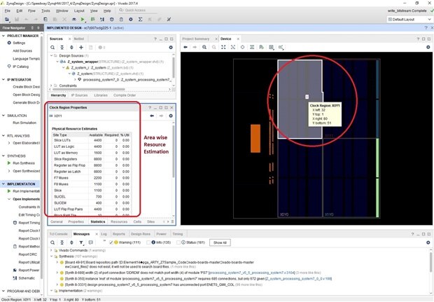
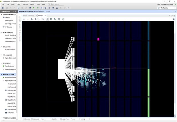
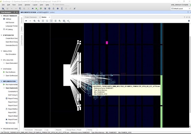
Floor planning of the chip
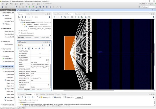
The connections on the FPGA
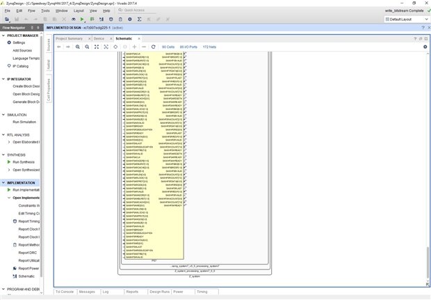
All the peripherals in the Zynq FPGA processing system
Lab 4
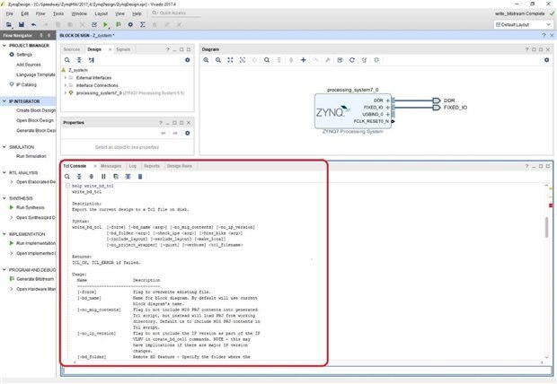
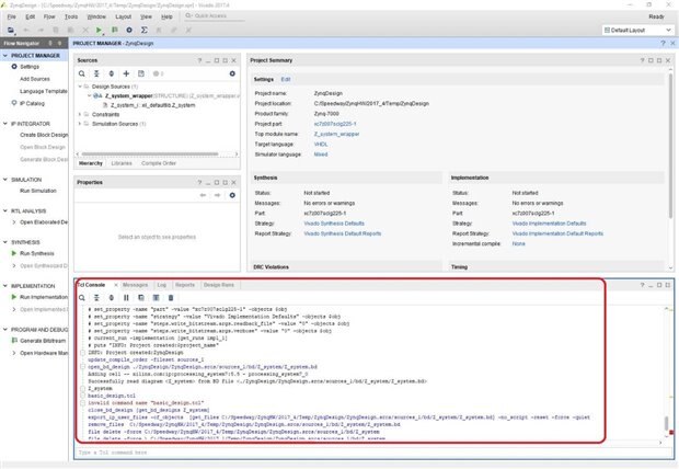
This lab is more focused on scripting and using scripts instead of the Vivado GUI to design the system. Tool Command Language (TCL) commands are important to understand as all Xilinx tools run TCL in the background system.
Lab 4 Objectives
• Open and close block designs using TCL
• Execute simple TCL commands to manipulate IP Integrator block designs
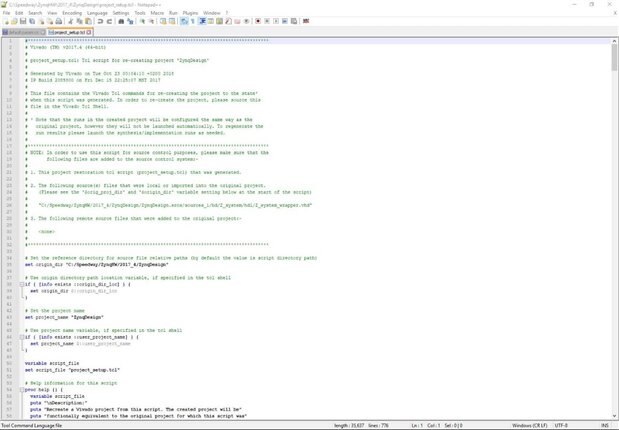
• Export a block design to a TCL file on disk
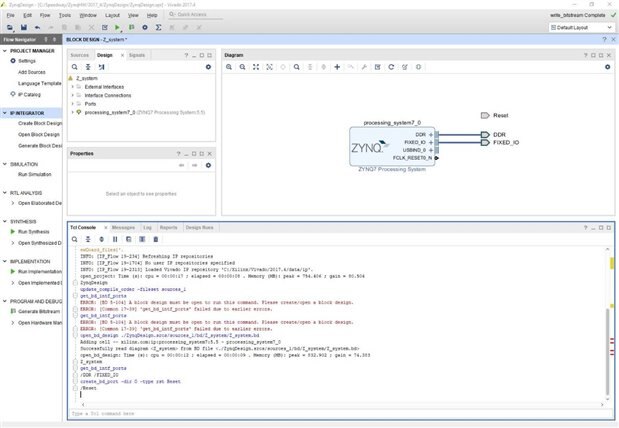
There is a long help menu to understand the scripting for Vivado. And the console is also very intuitive and help with commands completion.
project_setup.tcl script
Lab 5
In this lab, we expand the previous block design by extending the memory space with a PL-based Block RAM (BRAM). The BRAM is used to buffer data going between the PS and PL.
Lab 5 Objectives
• Add a BRAM from the IP Catalog
• Connect AXI peripherals to the Zynq PS.
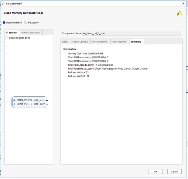
The BRAM (Block RAM Controller) is available in the IP Catalog as the AXI BRAM Controller. The 64 bit data width is adjusted in the AXI BRAM Controller IP settings options. Then using the automation connection wizard the Zynq PS (processing_system7_0) block is connected to the BRAM.
The updated block diagram
Summary of the BRAM Memory
The new connections established between ZYNQ and BRAM
Conclusion
The labs are well written. And not so difficult to follow as well. I found the TCL scripting part really interesting and handy. as for the rest; one has to self-investigate deeply further to learn what Vivado has to offer.





Top Comments
-

Fred27
-
Cancel
-
Vote Up
+4
Vote Down
-
-
Sign in to reply
-
More
-
Cancel
-

Fred27
in reply to Fred27
-
Cancel
-
Vote Up
0
Vote Down
-
-
Sign in to reply
-
More
-
Cancel
-

snidhi
in reply to Fred27
-
Cancel
-
Vote Up
0
Vote Down
-
-
Sign in to reply
-
More
-
Cancel
Comment-

snidhi
in reply to Fred27
-
Cancel
-
Vote Up
0
Vote Down
-
-
Sign in to reply
-
More
-
Cancel
Children