element14 Community
element14 Community
    Register Log In
  • Site
  • Search
  • Log In Register
  • About Us
  • Community Hub
    Community Hub
    • What's New on element14
    • Feedback and Support
    • Benefits of Membership
    • Personal Blogs
    • Members Area
    • Achievement Levels
  • Learn
    Learn
    • Ask an Expert
    • eBooks
    • element14 presents
    • Learning Center
    • Tech Spotlight
    • STEM Academy
    • Webinars, Training and Events
    • Learning Groups
  • Technologies
    Technologies
    • 3D Printing
    • FPGA
    • Industrial Automation
    • Internet of Things
    • Power & Energy
    • Sensors
    • Technology Groups
  • Challenges & Projects
    Challenges & Projects
    • Design Challenges
    • element14 presents Projects
    • Project14
    • Arduino Projects
    • Raspberry Pi Projects
    • Project Groups
  • Products
    Products
    • Arduino
    • Avnet Boards Community
    • Dev Tools
    • Manufacturers
    • Multicomp Pro
    • Product Groups
    • Raspberry Pi
    • RoadTests & Reviews
  • Store
    Store
    • Visit Your Store
    • Choose another store...
      • Europe
      •  Austria (German)
      •  Belgium (Dutch, French)
      •  Bulgaria (Bulgarian)
      •  Czech Republic (Czech)
      •  Denmark (Danish)
      •  Estonia (Estonian)
      •  Finland (Finnish)
      •  France (French)
      •  Germany (German)
      •  Hungary (Hungarian)
      •  Ireland
      •  Israel
      •  Italy (Italian)
      •  Latvia (Latvian)
      •  
      •  Lithuania (Lithuanian)
      •  Netherlands (Dutch)
      •  Norway (Norwegian)
      •  Poland (Polish)
      •  Portugal (Portuguese)
      •  Romania (Romanian)
      •  Russia (Russian)
      •  Slovakia (Slovak)
      •  Slovenia (Slovenian)
      •  Spain (Spanish)
      •  Sweden (Swedish)
      •  Switzerland(German, French)
      •  Turkey (Turkish)
      •  United Kingdom
      • Asia Pacific
      •  Australia
      •  China
      •  Hong Kong
      •  India
      •  Korea (Korean)
      •  Malaysia
      •  New Zealand
      •  Philippines
      •  Singapore
      •  Taiwan
      •  Thailand (Thai)
      • Americas
      •  Brazil (Portuguese)
      •  Canada
      •  Mexico (Spanish)
      •  United States
      Can't find the country/region you're looking for? Visit our export site or find a local distributor.
  • Translate
  • Profile
  • Settings
PiCasso Design Challenge
  • Challenges & Projects
  • Design Challenges
  • PiCasso Design Challenge
  • More
  • Cancel
PiCasso Design Challenge
Blog PiCasso Design Challenge - Kinetic Art Mobile - Post 5 - Finally a PCB design.
  • Blog
  • Forum
  • Documents
  • Polls
  • Files
  • Events
  • Mentions
  • Sub-Groups
  • Tags
  • More
  • Cancel
  • New
  • Share
  • More
  • Cancel
Group Actions
  • Group RSS
  • More
  • Cancel
Engagement
  • Author Author: genebren
  • Date Created: 2 May 2019 3:45 PM Date Created
  • Views 2229 views
  • Likes 14 likes
  • Comments 21 comments
Related
Recommended

PiCasso Design Challenge - Kinetic Art Mobile - Post 5 - Finally a PCB design.

genebren
genebren
2 May 2019

Prior posts in the PiCasso Design Challenge:

PiCasso Design Challenge - Kinetic Art Mobile - Post 1

PiCasso Design Challenge - Kinetic Art Mobile - Post 2

PiCasso Design Challenge - Kinetic Art Mobile - Post 3 - Will it go round in circles????

PiCasso Design Challenge - Kinetic Art Mobile - Post 4 - Crash of the Death Star


Things have been crazy here lately.  I have been very busy trying to finish out the interior of my new workshop, while attempting to keep my PiCasso project moving.  I have stuck in a re-design cycle, where I have been moving components from board to board, trying to get everything to fit, in a reasonable way.  After multiple re-starts on the design, I think I have a workable design.


There are several different requirements on the design that have made it fairly difficult to find the right approach.  Here are a few of them:

  • uniform LED spacing to allow proper illumination of the orb and to allow some 'animations' based on different LED color patterns and sequences.
  • relatively high power (LED and Fan power)
  • fan speed control (based on programmable constant current)
  • BLE transciever
  • Magnetic compass and accelerometer


I went through several trade off, trying to keep all of the high speed stuff on a single board, versus the space required for connectors should I distribute the components across multiple boards.  Here is what I ended up with:

imageimage

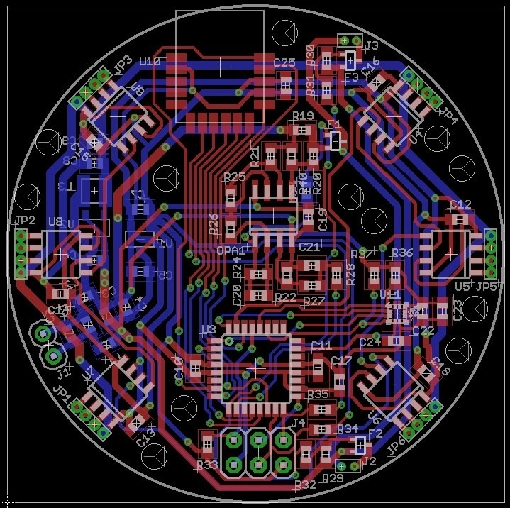
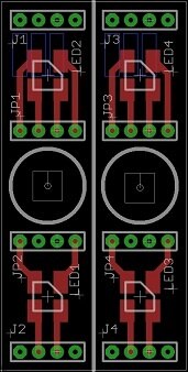
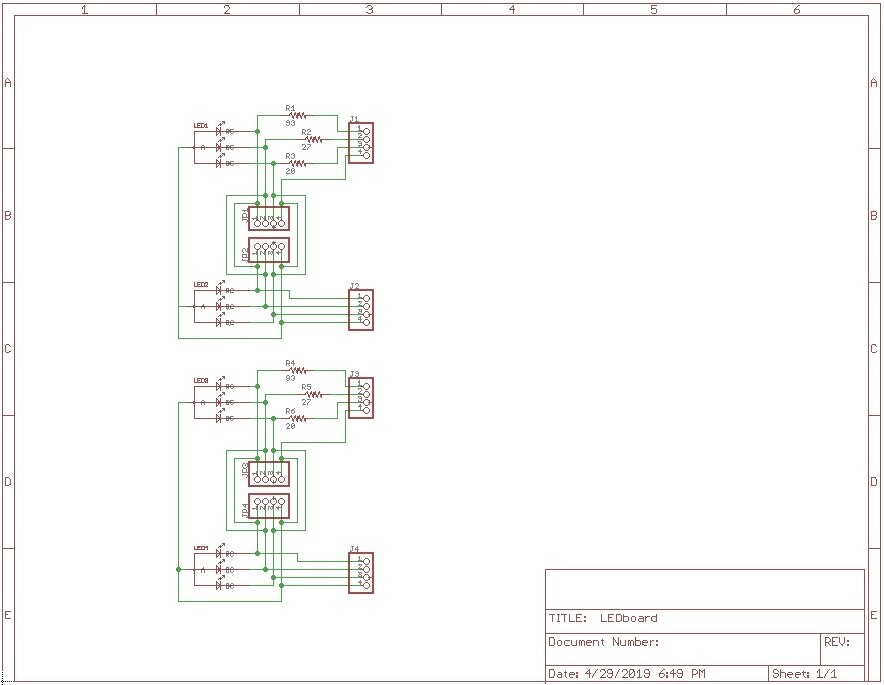
The Main PCB is riddled with 12 - 0.1" holes to allow additional air flow, through the board, into the fans below (there will also be some airflow around the board edges).  I will be trimming the PCB into a circle, as my PCB vendor (lower cost) only allows for rectangular boards.  The LED boards are sort of a universal design that will be connected to the main PCB, providing pairs of  LEDs along the circumference of orb and a single LED providing downward lighting (right angle mounted, hacked LED PCB).  This will provide me with 18 - fully programmable RGB LED to illuminate the sides and bottom of the orbs.


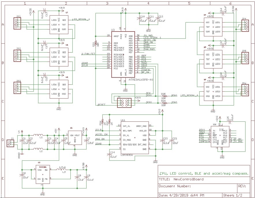
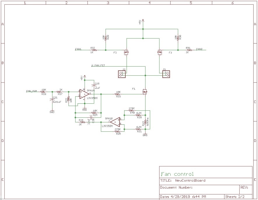
Here are the schematics of the main controller and LED board:

imageimage

image


I will need to send these boards of soon and order up parts for the board, but for now, I heading out to the workshop to install drywall and lighting.


Thanks for reading along.  I hope that I can get this project moving along a bit faster, so I can meet the deadlines.


Thanks,

Gene

  • Sign in to reply

Top Comments

  • genebren
    genebren over 6 years ago in reply to dubbie +6
    Thanks Dubbie. I have been laying out PCBs for quite a while (45+ years). I go back to self etched boards, using resist pens, tape or photoresist film (1970's), through many different design packages.…
  • genebren
    genebren over 6 years ago in reply to ralphjy +6
    Ralph, I do all of my assembly by hand (under a microscope). I do not have a reflow oven yet, but it is on my wish list for future tool purchases. The LSM303C (3D accelerometer and 3D magnetometer) is…
  • dubbie
    dubbie over 6 years ago +5
    Gene, Impressive PCB design. I've done a few simpler ones in my time but nothing like this. Dubbie
Parents
  • shabaz
    shabaz over 6 years ago

    Hi Gene,


    This is looking fantastic : ) It's nice that you're not afraid to change angles to get your components located where you want them : ) Regarding circle, the low-cost PCB manufacturers seem fine with routing out shapes, e.g. with the mouse-bites, so that could be an option too (i.e. lines on layer 46 in EAGLE). They do sometimes query via an e-mail to double-check they've got it right, so if you're on a timeline that's something to watch out for.

    For the LGA package etc., my pre-heater and hot air tool are underpowered, so recently I've thought about trying low-temp solder paste with it. I don't know if it will work though! I'll try it in a few weeks time, I'll be sending a couple of PCBs to be made in a week or so. The one I went for is called Qualitek Delta 670.


    Anyway, it's a really nice design and layout, it's clear a lot of effort went into it! It takes me days to route out stuff tidily.

    • Cancel
    • Vote Up +4 Vote Down
    • Sign in to reply
    • More
    • Cancel
  • genebren
    genebren over 6 years ago in reply to shabaz

    Thanks shabaz,


    I rarely change angles away from 90 degree increments, but in this case, in order to get the LED pointed correctly, I had to do at least the connector at an angle.  Once that was done, it did not make sense to have the connected ICs at a different angle, so they moved too.  It sure is strange routing traces away from the off angle components, back to my normal 45/90 degree traces.


    The LGA packages are going to be an adventure.  I has tried some leadless parts in the past, with varying degrees of success, so it is hard to predict how this will go.  I have put some serious thought into getting/building a small reflow oven just for these types of parts.


    Thanks again,

    Gene

    • Cancel
    • Vote Up +5 Vote Down
    • Sign in to reply
    • More
    • Cancel
  • shabaz
    shabaz over 6 years ago in reply to genebren

    I laid out a 32-pin LGA a couple of evenings ago (some clock part for my old DDS project) and for any 0.5mm pitch although I guess it isn't best practice (I don't know : ( but personally I switch off the tStop and tCream layers, and do them manually (i.e. so that the overall design rules don't apply). That way, I can get a bit of solder mask in-between the pads (although it can arrive broken! the low-cost manufacture seems to not be able to do the mask in-between reliably especially at 0.4mm pitch, but 0.5mm is just-about feasible I hope).

    Like you, I have variable results, I'm confident of the pasting and positioning, but I suffer from low-power heat sources : (

    With the low-temp solder I'm going to try to get nearly all heat from the pre-heater, so that the hot air gun is barely (or not) needed.

    image

    • Cancel
    • Vote Up +4 Vote Down
    • Sign in to reply
    • More
    • Cancel
  • genebren
    genebren over 6 years ago in reply to shabaz

    Thanks shabaz.  That is a good tip on manually applying the cream/stop to the footprint.  I did a quick update on my PCB to shrink the rectangles to provide a minimal stop between the pins.


    Thanks again,

    Gene

    • Cancel
    • Vote Up +5 Vote Down
    • Sign in to reply
    • More
    • Cancel
Comment
  • genebren
    genebren over 6 years ago in reply to shabaz

    Thanks shabaz.  That is a good tip on manually applying the cream/stop to the footprint.  I did a quick update on my PCB to shrink the rectangles to provide a minimal stop between the pins.


    Thanks again,

    Gene

    • Cancel
    • Vote Up +5 Vote Down
    • Sign in to reply
    • More
    • Cancel
Children
No Data
element14 Community

element14 is the first online community specifically for engineers. Connect with your peers and get expert answers to your questions.

  • Members
  • Learn
  • Technologies
  • Challenges & Projects
  • Products
  • Store
  • About Us
  • Feedback & Support
  • FAQs
  • Terms of Use
  • Privacy Policy
  • Legal and Copyright Notices
  • Sitemap
  • Cookies

An Avnet Company © 2025 Premier Farnell Limited. All Rights Reserved.

Premier Farnell Ltd, registered in England and Wales (no 00876412), registered office: Farnell House, Forge Lane, Leeds LS12 2NE.

ICP 备案号 10220084.

Follow element14

  • X
  • Facebook
  • linkedin
  • YouTube