


Table of Contents
Introduction
Greetings Dear Reader,
I have written this blog in response to the "Summer of FPGA" challenge, and being my first blog on the platform I wanted to describe my experience with the Digilent CMOD S7 board before going into making my LiFi project come to life.
This is also my first time using an actual living (not really) breathing (also not really) FPGA. Even though I studied Logic Design using HDL in college I never actually got into hardware implementation. I will be using Verilog as my HDL throughout and discuss a few concepts along the way.
Getting Familiar with the Board (CMOD S7)
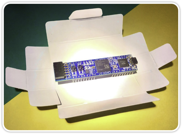
is a development board hosting a Xilinx Spartan 7 (XC7S25-1CSGA225C) FPGA, tighly integrated with the appropriate number of onboard LEDs and buttons while exposing the rest of the IO via the 4x 7 DIP headers. Additionally the, board comes with a PMOD connector, USB port, and a SPI flash.
Interfacing with the board is generally done through USB, interfaced via an onboard FTDI chip (located close to the USB).
The board is comes packaged with a triple output buck power regulator capable of supplying three different voltage levels. The FPGAs clock is run by a 12MHz external crystal oscillator.
I won't go into listing all the features of the FPGA chip here at once, instead I will be referencing them throughout the blog. Nonetheless, the official digilent reference manual can be found here
-
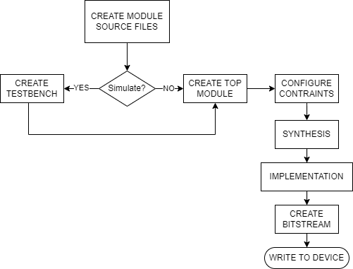
First we create or include the source files using your HDL of choice.
-
If there is a need to simulate the design then we would have to create a testbench and set it as the simulation top file (this is like the int main() of an HDL project).
-
Otherwise we can simply create the top module which encapsulates all the modules and defines connections between them.
-
Next, we configure the constraints for the design, this includes things like pin mapping, base clock configuration, etc. Using the
.xdcfile. -
Synthesize the design into a workable schematic.
-
After synthesis, we must run an implementation which describes the synthesized circuit in terms of the FPGA's resources.
-
We must now write the implementation into a bitstream which is analogous to a hex file that would be sent to a microcontroller.
-
Finally, we program the device.
Xilinx FPGAs implement logic designs using SRAM which is volatile, meaning the device resets on loss of power. These FPGAs utilize LUTs (Look-up tables) which can be thought of as hardware truth tables made up of SRAM cells. The floorplan of the chip consists of cells called CLBs (Configurable Logic blocks) made up of LUTs and connected using interconnection matrices called "magic boxes" which establish connections using transistors as switches.
Setting Up Vivado

Xilinx provides a free-of-cost version of called the WebPack edition of their Vivado Design Suite. It consists of a comprehensive set of tools required for HDL designs. However it must be noted, that while the installer does support post installation compression it is still a large download and does require a comparatively fast PC.
I initially thought it would be difficult to get used to the GUI however, I couldn't have been further from the truth. From creating a project to navigating the project directory, everything was simple and natural. It took about 10 mins for me to get used to most of the interface and that mostly includes load times. Even including device libraries were easy to follow.
Installing Board Files
Speaking of libraries, while Vivado comes preloaded with board and chip libraries, the CMOD S7 had to be included by me manually. To check whether it is installed:
-
Open Vivado
-
Create a project
-
Add a temporary project name and click
next -
Choose RTL synthesis (Register Tranfer Logic) and click
next -
Finally it comes down to selecting the board, click on the boards tab and search for
CMOD S7
If it doesn't show up then it must be included manually. Follow the steps below or consult this link:
-
Clone this GitHub repo
-
Open the repo directory and navigate to
new/board_filesand you may either copy all or select the directory -
Now paste the folder into
Note: the ${XILINX} filepath is different for different operating systems
-
Once done, restart or open Vivado, and you should see
CMOD S7under the boards section.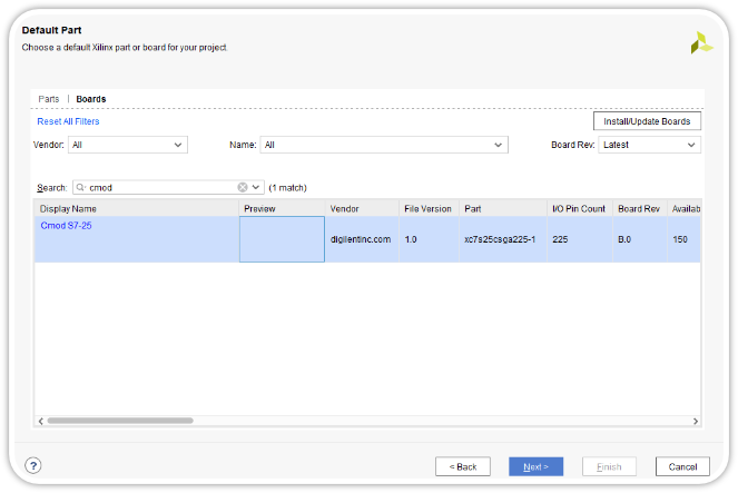
nextandFinish
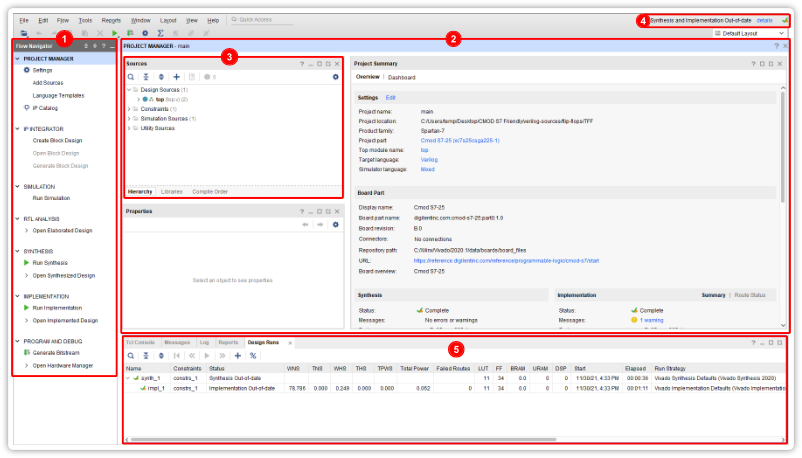
On opening a project file, you would be greeted by the screen above. I have divided the screen into zones that would be referenced later. They are as follows:
-
[Zone 1]: This is the
Flow Navigator, it consists ofTabssectioned for design processes like synthesis, implementation, simulation, etc. -
[Zone 2]: I shall refer to this zone as
Mainas it changes depending on the flow stage selected. For eg: if you were to select implementation then it would show you things like device footprint, floorplan, schematic, etc. -
[Zone 3]: Here we see our
Sourcespanel, where we may add, delete, or assign source HDL files required by the project. -
[Zone 4]: The
Process Indicatorcan be easily missed at first, its purpose is to provide visual feedback about the running status of a task. In other words, its a loading widget. -
[Zone 5]: This will be referred to as the
Reporter, as it shows things like logs, messages and other similar information. Just likeMainit too changes depending on the selected section.
Structural HDL
Essentially There are three design methods in HDL that govern the approach for a problem:
-
Structural
-
Dataflow
-
Behavioral
Structural HDL requires you to describe the logical circuit, this also includes defining interconnection between each stage in the logic circuit. In other words, you must define the structure of the circuit.
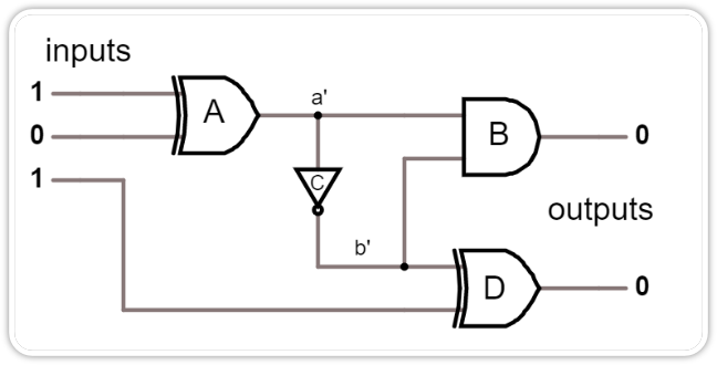
For example, If we want to create the circuit above, we must define the 3 inputs and 2 outputs, and then separately define each gate connected by wires. We can observe that a' connects gate A to gates C and B, similarly b' connects the output of C to B and D, these "lines" or "nodes" must be defined in HDL as wires.
From this example it is easy to understand why the structural model of HDL alone becomes quite complex, and therefore requires alot of planning in order to execute properly. Tracing issues may also be time consuming.
However, When it comes to describing a logic circuit directly from its structure then structural is chosen. Nonetheless scaling of a design is much more difficult and requires multiple levels of abstraction in order to tame its complexity.
Revisiting Gates
As an introduction to structural HDL I decided to go for the implementation of basic gates.
Since a hybrid of behavioral and structural are necessary for most of our designs, and the use of structural alone is sparse in the practical FPGA development.
Below is the template for the module:
module gen_gate (output out, input x, y);
    and(out, x, y); // <- line one
endmodule
line one
-
not(out, x)remember to remove the other input from the ports list -
OR:
or(out, x, y) -
NAND:
nand(out, x, y) -
NOR:
nor(out, x, y) -
XOR:
Let's implement these gates in the CMOD shall we!
Let's first open up a Vivado project, and add some sources using the sources panel:
-
click on the
+button
- next, check the
- now click on
Create File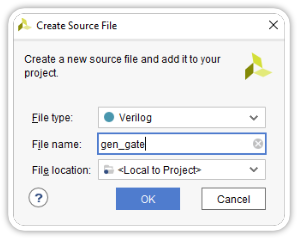
- make
Verilogis selected and the file name is same as the module, and click - press , and an IO definition box should appear, however we aren't going to be following this wizard, instead we will add these pins via the
.xdcfile. Therefore press - in
.xdcfile of theCMOD S7. XDC files are constraint files that describe what all peripherals the FPGAs pins are connected to. You may find the.xdcfor theCMOD S7from here - before
.xdcfile you downloaded earlier and add it to yoursourcesusing theAdd or create constraintsoptions in the wizard similar to how we added the verilog source but for an XDC instead. It should now show up in the Constraints section of thesources - open this file, and you will notice that the pin names are clearly stated after
PACKAGE_PINS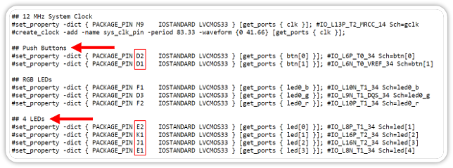
- Do the same for the other buttons and the LED and save.
Notice the LCVMOS33 in the .xdc definitions, these indicate the power level. The CMOD S7 comes with a power regulator (LTC3569 triple output buck regulator) capable of supplying 3 voltage levels. These are as follows:
-
3.3V
-
1.8V
-
1.0V
-
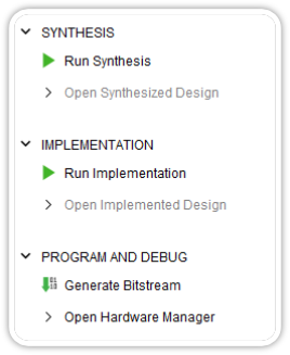
- now
Flow Navigator 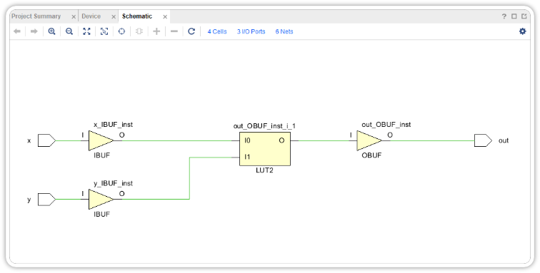
- If
- Now
CMOD S7to the computer and underPROGRAM DEBUGinside theOpen Hardware Managerdropdown click onOpen Target>Autoconnect - Once
Program Deviceand select the board.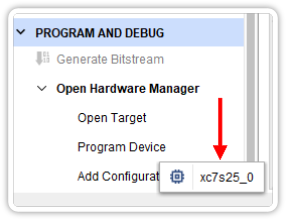
- And there ya go! your FPGA AND gate is complete.

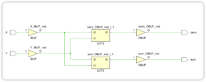
Half Adder
Let's try something a little more complex, again without using any additional hardware and instead relying solely on the board's peripherals.
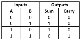
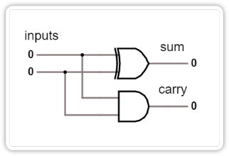
Directly moving on to the verilog module file, we require:
-
-
2 outputs - sum and carry
-
connect X and Y to a XOR gate and call its output sum
-
connect X and Y to an AND gate and call its output carry
The verilog module will look like so:
module half_adder (input X, Y, output sum, carry);
    xor(sum, X, Y);
    and(carry, X, Y);
endmodule
And that's it! now just map the required pins that is the 2 onboard LEDs and the 2 buttons - synthesize implement and generate the bitstream. Let's write the bitstream to the device.

And the schematic for the same looks something like this:
Cell Properties within the Main
 As mentioned earlier the circuit has a intermediate stage where the NOT gate comes in between one of the input and the AND gate, What to I do here? How do I map the pins? Well first of all ... Simmer down. We must create an internal wire connecting the NOT output to the input of the AND gate. Remember
 wires are a type in verilog that can be connected to unlimited inputs but have only one output, this is so that multiple signals don't converge on the same spot. Let's take a look at the verilog module shall we:

What's next?
Initially I wanted to include the behavioral model as well and directly transition to using the core IPs provided by Vivado while also simultaneously exploring the Vitis IDE, however, that would have taken a lot more time and would be rather long. So instead I would like to invite you to my upcoming (or already up) blog on the behavioral model of HDL along with a possible introduction to Tcl scripting. Along the way I will also publish a repo containing the necessary example files. So until then I hope to meet you in the next one.
-

kluivertcorreia
-
Cancel
-
Vote Up
0
Vote Down
-
-
Sign in to reply
-
More
-
Cancel
Comment-

kluivertcorreia
-
Cancel
-
Vote Up
0
Vote Down
-
-
Sign in to reply
-
More
-
Cancel
Children