LiFi #2 - Behavioral Modules
Table of Contents
-
Abstract
-
Clock Dividers
-
Counter based
- fixed
- generic
-
Clocking Wizard IP
-
-
Counters
- BCD counter
- Johnson's counter
-
Conclusion
Abstract
In this blog I've decided to give a "small" intro to behavioral HDL, before moving to the sequence detector which will be used in framing for LiFi. We will first look into creating a simple counter based clock, then move onto a few examples of counters just to play with the clock a bit.
I also hope to keep this one shorter
Clock Dividers
Sequential devices require a clock to run. The clock is necessary for carrying out state based actions i.e., actions based on past and present inputs/outputs. In its simplest form a clock outputs a square wave, toggling from LOW to HIGH.
The CMOD S7 is driven by a 12MHz external clock, which is plenty fast for our application however running logic that counts at that speed is obviously not fun. Therefore, we must divide the clock by some amount to observe it.
Xilinx provides a Clock Wizard IP that can configure the clock for our design, however I would prefer to show a counter based clock using verilog and then go for the wizard which would use the MMCM (Mixed Mode Clock Manager) module driven by the 12 MHz clock to give our desired output clock by either multiplying or dividing the input frequency. There is also a provision to use the PLL (Phase Locked Loop) however the reference manual suggests that this is not possible due to the minumum input clock frequency of 19 MHz.
Counter Based
This kind of clock divider works by simply counting up till a predefined limit during which is toggles the output clock level and resets the counter.

First let's set the simulation bench:
`timescale 1ns/1ns

// simbench

module simbench;

reg in_clk = 0;
wire out_clk;

// wrapper module
clk_divider wrapper(
.clk(in_clk),
.out_clk(out_clk)
	);

// simulate the 12 MHz clock
// toggle every 42 ns
always #42 in_clk = ~in_clk;

endmodule
We can observe the timescale set to 1ns, this resolution is fine for our simulation requirements and since the time period for 12 MHz is 42ns we create a toggle event triggered using always.
Now for the top module to finalize our hardware implementation:
// testbench

module top(
input wire clk,
output wire out_clk
	);

// wrapper module
clk_divider wrapper(
.clk(in_clk),
.out_clk(out_clk)
	);

endmodule
Fixed
We shall simplify our task by creating a clock source with a period of 200 ms (100 ON + 100 OFF, 5 Hz). Let's take a look at the source file observe the different sections:
// clock divider module (fixed)

module clk_divider(
input wire clk,
output reg out_clk = 0
	);

localparam LIMIT = 1200000; // count until
integer counter = 1;

always @(posedge clk) begin
	if (counter == LIMIT) begin
		counter = 1;
		out_clk <= ~out_clk;
	end
	else
		counter = counter + 1;
end

endmodule
localparam stands for local parameter, we will be revisiting a more useful form of this later. Here the LIMIT is set to 1200000, so the counter would count until this LIMIT and reset and toggle the output clock. The counter is of type integer which in verilog is 32 bits long.
We can calculate the limit using the following expression:

here our input frequency is 12 MHz and out output frequency is 5 Hz which gives us the aforementioned LIMIT value.
Running the simulation, results in the following waveform:

As you can see its working, so let's finalize the design by synthesizing the top module.
BUT before all of that, we must configure the XDC constraints file by routing the input clock to the external clock and the output clock to one of the onboard LEDs.

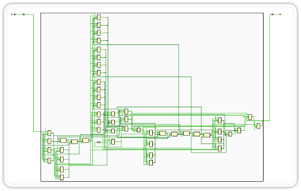
This shows the block diagram from the top module, we can reveal the wrapper block internals by double clicking on it or clicking on the '+' button.


Obviously, the 32 bit counter comes with a price, of propagation delays, complexity and space usage, but as an introduction to clock dividers it qualifies as gateway for beginners.
Finally after Synthesizing, Implementing, Generating Bitstream and programming the FPGA we obtain this boring show .

Generic
Fancy a change! Now we will give the verilog file the ability to become configurable. We can do this by using parameters in verilog. The clock divider module will have an additional parameter list of type parameter, it is structured as follows:
module <module_name> #(parameter <par_name>, ...) (<port_list>);
    ...
endmodule
As seen below the parameter list is indicated using '#'. We can also give the parameter default values which are used in case it is not configured during instantiation. With that in mind the clock divider module will look like this:
`timescale 1ns / 1ns
// clock divider module

module clk_divider #(parameter LIMIT=6000000) (
	input wire clk,
	output reg res_clk
	);

integer counter = 1;

initial res_clk = 0;
always @(posedge clk) begin
	if (counter == LIMIT) begin
		counter <= 1;
		res_clk <= ~res_clk;
	end
	else
		counter <= counter + 1;
end
endmodule
This can be directly used by our previous top module however, to define parameters ourselves we need to use the defparam keyword and refer to the target module using the '.' symbol.
defparam <target_module>.<par_name> = <value>; // after instantiation
We shall configure the top module to include a fast clock and a slow clock.
`timescale 1ns / 1ns
// Top module

module top (
input wire clk,
output wire slow,
output wire fast
	);

// create slow_clk
clk_divider slow_clk (
.clk(clk),
.res_clk(slow)
	);

// create fast_clk
clk_divider fast_clk (
.clk(clk),
.res_clk(fast)
	);
defparam fast_clk.LIMIT = 400000; // set the LIMIT
endmodule
Set the constraints for the fast and slow outputs as LEDs and finally Synthesize, Implement, Make bitstream and Program or SIMP for short (I know I cheated with this one) and you will see it working.


Clocking Wizard IP
An IP (intellectual property) are generally modules packages by a firm to be plug and play, they follow a configuration wizard and then get built into a file that can be instantiated by the designer in other modules.
Xilinx FPGAs have the ability to create clock sources using a PLL (Phase Locked Loop) or MMCA (Mixed-Mode Clock Manager), these usually need some time to lock into a frequency and have the capability of not only dividing the frequency but also multiplying it to a certain extent. The IP provides additional control signals to provide more information about the clock source.
Without a good oscilloscope, I won't be able to observe the output frequency (maybe possible through some assembly optimized bare metal code on a fast enough microcontroller but that is too much work for a small demo), So instead I will be using the simulator to simulate the input clock.
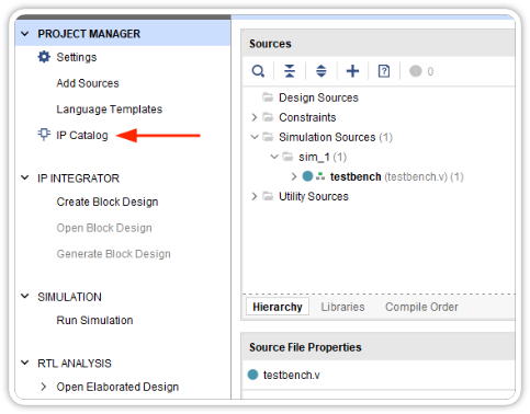
To use an IP you need to head over to the IP Catalog:

It will open panel showing all the available IPs, search for "Clocking Wizard" and select it:

Now you will be greeted with a configuration window showing a block on the left pane and the various option on the right:

Here I changed the "Component Name" to clock_source, next click on the "Clocking Options" tab:

Set the Primitive to MMCM, the input frequency to 12 MHz and while we're at it change the port name. Notice the number range besides this box, this indicates the input frequency range limit, it is different for PLL. More information about clocking can be found from the Spartan-7 FPGAs Data Sheet under switching characteristics.
Now Let's move on to the "Output Clocks" tab:

Set the output clock frequency to 24 MHz. I have removed the reset port and kept the locked port. The locked port is a control signal that indicates whether the output clock has stabilized or "locked" with the desired frequency.
Finally "OK" to complete the wizard and "Generate" using the default options, you will see the module in the sources panel.

You may have noticed the testbench file there. The created module also includes a template for instantiating the clock_source, we can find it in the "IP Sources".

open the highlighted .veo file and you will find a template for instantiating the clock_sources module. Finally the testbench file will look a little something like this:
`timescale 1ns / 1ns
// testbench module

module testbench;

// define ports
reg clk = 0;
wire res_clk, locked;

// create the 12 MHz input clock
always #42 clk <= ~clk;

// create the wrapper
clock_source wrapper (
.clk(clk),
.res_clk(res_clk),
.locked(locked)
	);
endmodule
Notice we have to manually create an input clock source in order to drive the simulation. Running the simulation would give us the following waveform:

The total simulation time was 100 µs, we can immediately notice the locked signal taking a bit of time to go HIGH meaning the output clock gets synced to the set frequency at that time. Zooming in we notice the frequency multiplication as the time period for our output clock signal is half of our source signal.

If you want to implement this in hardware then instead of creating a pulse explicitly, you would need to configure the constraint file to use your external clock as input and maybe route your output through one of the IO pins.
Counters
Implementing a counter on a dev board is a satisfying exercise, even though the CMOD S7 boots with a counter on the 4 onboard LEDs.
BCD counter
A BCD counter essentially counts digits i.e., 0-9 in binary and then resets. Implementing a circuit in behavioral verilog is quite easy and intuitive. First make sure you have a clock divider so that we can observe the counter, for this I will make use of the generic clock we designed earlier and the bcd counter module would contain:
// BCD counter module

module bcd_counter(
input wire clk,
input wire reset,
output reg [3:0] dout
	);

initial dout = 0;

always @(posedge clk or posedge reset) begin
    if (reset || dout == 9)
		dout <= 0;
	else
		dout <= dout + 1;
end
endmodule
Here we wait for a rising edge clock or a rising edge reset and branch if the reset is high otherwise count dout up until we reach 10 after which we reset trigger a reset. The top module is pretty straightforward in that we propagate the external clock of the CMOD S7 to the clk_divider module and then use it's output to drive the counter.
// Top module

module top(
input clk,
input reset,
output [3:0] dout
	);

wire res_clk; // used to drive the counter

// create the clock wrapper
clk_divider runner(
.clk(clk),
.res_clk(res_clk)
	);

// create the counter wrapper
bcd_counter wrapper(
.clk(res_clk),
.reset(reset),
.dout(dout)
	);
endmodule
you know the drill, configure the constraint file and SIMP, The result is:

Johnson's counter
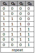
The Johnson's counter is just another exercise for a sequential circuit. The output sequence is as such:

We can deduce an equation or algorithm for the next state by simply looking at the above excitation table. Here we notice that the next state can be written as the current state shifted right by 1 and the negated value of the rightmost bit is set as the first or leftmost bit of the next state. We can see this in action below.

Now Let's create the module:
// Johnson's counter module

module johnson(
input wire clk,
input wire reset,
output reg [3:0] dout = 4'b0000
	);

reg msb; // holds the rightmost bit

always @(posedge clk or posedge reset) begin
	if (reset)
		dout <= 0;
	else begin
        msb = ~dout[0];
        dout = (dout >> 1) | (msb << 3);
	end
end
endmodule
Implement it in the top module like so:
// Top module

module top(
input clk,
input reset,
output [3:0] dout
	);

wire res_clk;

clk_divider runner(
.clk(clk),
.res_clk(res_clk)
	);
defparam runner.LIMIT = 3000000;

johnson wrapper(
.clk(res_clk),
.reset(reset),
.dout(dout)
	);
endmodule
Finally set the constraints and SIMP.

Conclusion
In this blog I have discussed the use of the behavioural model for FPGA design using Verilog, in the next one we will look towards making a generic 4 bit sequence detector required for framing purposes in the final LiFi design. Thanks for following along and I hope to meet you in the next one.

-

DAB
-
Cancel
-
Vote Up
0
Vote Down
-
-
Sign in to reply
-
More
-
Cancel
Comment-

DAB
-
Cancel
-
Vote Up
0
Vote Down
-
-
Sign in to reply
-
More
-
Cancel
Children