LiFi #4: Custom LiFi Peripheral
Table of Contents
Abstract
As promised in an earlier edit, this is the UPDATE I wanted to make to give a more comprehensive overview of the whole project.
My plan for this blog is to explain my thought process behind a few of the design decisions I made and a high level abstraction of the design itself. Ideally I would have wanted 2 FPGAs to enable simultaneous two way communication, however I have to make use of what I have, so I decided to make things more difficult for me by designing the peripheral for the purpose of reception (because transmission is easier ). This is not to say that the peripheral can't transmit, it can, but since I have only one FPGA and more importantly four more days to submit I decided to make the ESP32 the transmitter and make the CMOD S7 a receiver tasked with the job of decoding and unpacking the packet.
My original plan suggests the use of two different wavelengths of light, specifically IR and visible light and that is exactly what I intended to do.
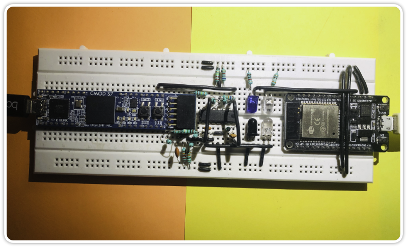
So without any further ado, I give you the custom LiFi Peripheral. Here is a small teaser of the end project.

Protocol
The protocol governs the format of the packet and defines the flexibilities, that may be used to customize a packet. The two LEDs could be thought of as two wire communication. But I take advantage of the specificity of the wavelength to filter one signal over the other as you will see soon.
Inspiration
There were 4 days remaining, however I took my time to design the protocol. At first I wanted to emulate i2C however I felt there was a better one, introducing CAN (Controller Area Network). After just a single YouTube video, specifically this one. The robustness of the CAN bus is what appealed to me, I immediately started to pen down a rough frame format and signaling rules to build my own.
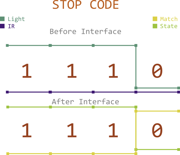
One important thing to mention is that I mapped the recessive and dominant signals to LED interface using two ports: MATCH and STATE. Here MATCH denotes that both the LEDs are the same state. STATE on the other hand is equal to the state of either the visible light or the IR, in my implementation I chose visible. Having two signals like this enables false signal detection, i.e. an unwanted signal like an IR remote signal or very bright ambient light can be detected and flagged.
Framing
The first task was to simplify the frame, this is to lower the number of modules required to process the frame later in order to lower the time taken to develop them. This is the frame that I came up with:

Comparing this to the CAN bus frame:
You can observe that I removed a few fields to simplify the process. The RTR (Remote Transmission Request) was not relevant to the final demo so I yeeted it. Similarly the ACK (Acknowledge flag) was removed as well. I wanted to keep the CRC block since I thought it would be a good exercise in error detection, and spoiler alert: IT WAS!
I also decided to use the entire 128 bit space in the datafield defined by the 4 bit length code that provides information about the length of the data in bytes.
Boundaries
The boundaries (START and STOP) are defined by a 4 bit sequence that makes use of both the MATCH and STATE. These sequences are detected using the sequence detector from blog #3. Other than just extracting data from the packet, the peripheral must also characterize the packet by extracting length data, ID, error flags, CRC error detections and so forth, these signals are exposed using registers.
START boundary:

STOP boundary:

Here the STATE defines the binary code BUT the MATCH validates the STATE otherwise ignores the code. For example, in the START code the MATCH equals the STATE whereas in the STOP code the MATCH is the complement of the STOP. The code itself is not a well selected one however at the time I was more concerned about the rule rather than the code itself. This sequence is adjustable in the module due to the generic nature of the sequence detector from blog #3, in fact in my implementation I didn't have to change the sequence from 0001 to 1110, I just inverted it which saved a lot of time.
All the blocks that come in between the START and STOP detector make use of only the STATE wire and validate the signal using MATCH, i.e. the IR and light must follow each other or it would raise a false_signal_error flag which will be explained in detail in blog #5.
Frontend Circuit
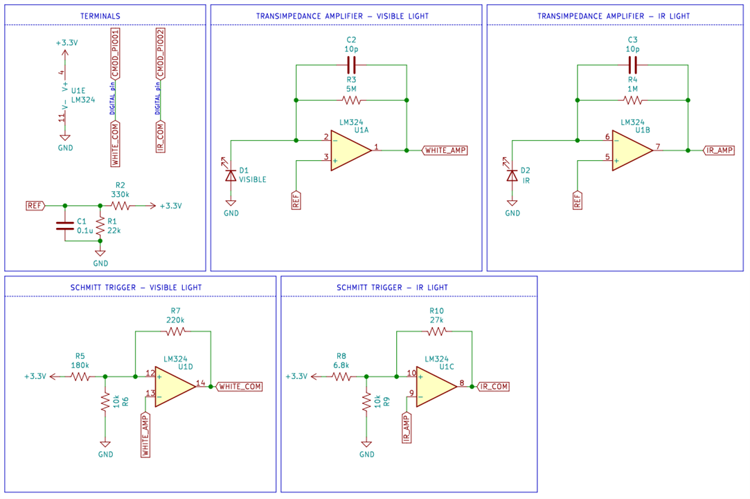
We need a way to convert the analog signal from the photodiodes to a digital one, here is where the frontend circuit comes in. The frontend circuit amplifies the current draw from the photodiodes and then defines trigger points to create a digital signal which can be fed to the CMOD S7. Due to lack of time (again 4 days) I couldn't purchase the required precision components, so I decided to use a normal 3mm green LED to act as a photodiode for visible light and an IR LED for the infrared light.
Originally, the circuit was also supposed to have a gain control which the protocol could also implement, in fact, I later opted to keep the gain fixed and instead change the trigger points or rather select the trigger points, however in favor of simplicity I decided to do no such thing and kept it in the background for later.
The circuit looks like so:

The transimpedance amplifiers are adjusted such that it would work at any time of the day in my room without getting affected by IR from sunlight. the lower and upper cutoffs are adjusted for greater response while also providing good enough buffer for different times of day. I ended up putting all of this on my breadboard along with the FPGA and the ESP32 testbench, so everything is extremely compact and fixed. I tested the transimpedance amplifiers separately using some analogRead test code, confirming the reading using a multimeter, and committing the calculated values for most of the components. Also observe that the entire design uses a single OP AMP IC.
Limitations
It should be noted that since I used a general purpose OP AMP (LM324) IC I had to make a few considerations in the design, one being the bypass capacitor, adding this capacitor defines a Low Pass Filter, in ideal conditions the -3dB point is at 3.21kHz however when considering the internal capacitance of the LED and the parasitic capacitance as a consequence of making the circuit on the breadboard, we can expect a much lower cutoff.
To make things worse, the Schmitt trigger thresholds now have to change to accommodate the lower amplification as a result the whole system has a very low bandwidth. However, my aim is for the custom LiFi peripheral to be able to decode the packet with high accuracy and robustness even if the bitrate defined is lower. In the end on testing, the device was able to sustain a 5ms period or 200Hz driving clock (this defines the internal clock which in turn defines the bitrate).
Design Flow Overview
Now I want to discuss my plan that I executed to get the device up and running.
- At first, I decided on a method of interface, i.e. MATCH and STATE signals.
- Then I developed a rough protocol to which I manually described a packet and recreated the packets on a ESP32 testbench which would serial out various fields and construct the packet.
- I made minor adjustments to boundary rules and committed to it.
- I collected and/or salvaged a few components for the frontend circuit.
- I implemented the frontend circuit and spent time tuning and testing it during different times of the day, while parallely designing a handwritten block diagram for the de-framing.
- I then decided on the registers that would be interfaced by the softcore.
- To create the transmitter I created a testbench using the ESP32 board and the Arduino framework over PlatformIO. This code handles the construction of the signal but could set a fixed message defined during compilation.
- After the block diagram was decided, I started writing the HDL in Verilog for the various modules (which will be discussed in the next blog).
- Each and every module was tested using a simulation testbench and some like the interface module were tested on the CMOD itself.
- Next I needed to combined and connect all the modules, so I decided to go for block design, HOWEVER this was the first MISTAKE I made. Not to be rude to whoever developed the update hierarchy of Vivado, but the update hierarchy sucks! Any changes done in block design would take nearly 45 mins which mostly included retries because the net references would never get updated. A combination of elaborating and just plain ol' waiting seemed to solve the issue. In most cases, I straight up recreated the whole circuit, which was not ideal since I was in the process of developing it in the first place.
- Finally, I decided to take the time to combine the individual modules in Verilog itself and develop a single module that I would be imported into the final block design with the softcore. And this quite literally was the biggest time saver of them all, as a result I was able to submit the project just before the deadline. It would take around 20 seconds to synthesize after an update verses the nearly 45 mins to 1 hour time on block design.
- Arrangement of code of such a complex module is very important. I created code fences for internal wires and registers in the beginning, then I followed through arranging all the modules by flow of data, i.e. from the START to ID to LEN to DATAFIELD to STOP and so forth. After this I created code fences for the registers and finally fences to the dataflow assignments and register events. After making most of the connections I noted all the potentially ambiguous signals that may be caused due to concurrency.
- Noting all these issues I created temporary changes to individual modules and create extra wires to run them.
- I made a powerful test bench called full_block_test to run all the possible combinations for packet type and errors are so forth. I ran the complete peripheral through the behavioral simulation and saw that it worked on the first try, however on close inspection and a error filled input sample I noticed some inconsistencies with signaling among modules. After many revisions are rewrites of certain processes I was able to get it to work consistently, however there were a few possibly issues that would come up in certain scenarios mostly to do with the boundary and clear or reset commands. I decided to spend a little more time on reviewing these signals and create test samples that would break it.
- I then manually defined the circuit graphically on paper and made a few optimizations after which I tried to fix those test samples that would cause the process to break. These signals were mainly the clear commands. Specifically the entire module has two internal clears: pre_clr and common_clr. The pre_clr handles clearing of buffers such as the datafield and received_ID register, while the common_clr handles resets of the other modules and is also responsible for reset the state for the next transaction.
- Once the simulation looked good enough I created the final block design. Here I added the MicroBlaze core with 128kB flash (which is required for xil_printf to work) and mapped each of the peripheral registers to the AXI GPIOs, I should mention at this point, that I had just started using the softcore and couldn't figure out how to interface the core with the peripheral, however with some help from YM Labs andnavadeepganeshu, I figured a simple solution using the AXI GPIOs. I had to divide the datafield into 4 AXI modules due to the 32 bit limit so the block diagram got a bit cluttered as a result.
- For debugging purposes I added additional constraints to expose the IR, light, ID match, START, and STOP signals using the onboard LEDs.
- To run the slow clock I used the generic counter from blog #2 to divide the 100MHz clock accordingly and fed it to the custom LiFi peripheral.
- Finally to Vitis, something that I deeply hate about the entire process but will discuss later. Here I wrote the demo code using all the registers of the peripheral and configuring it to read. Initially during my first edit of blog #5, I used a very simple testbench that wouldn't even translate the 128bit datafield, since at this point I closing in on the deadline. So it just showed the number saved in the first datafield register, this was because of the earlier revision of the ESP32 testbench wherein I could send a fixed message during compilation time. This message was a simple 'K', after some manual number crunching you could see that the data was indeed correct.
- After submitting the blogs however I decided to finish of the testbench and the demo which is the result of the CURRENT edit.
- And we're done! other than a few more tiny optimizations to the code after I am now satisfied with my MVP (Minimum Viable Project).
Conclusion
Its amazing to see how much I packed in those 4 days, the idea essentially just working on the first try was such a huge relief and close calls with the deadline has truly given me an adrenaline rush. However I may develop the project further with the help of *cough cough* measuring instruments .
Anyway thanks for tuning in!
And DON'T FORGET TO SMASH THAT LIKE BUTTON & COMMENT BELOW ON WHAT ARE YOUR THOUGHTS ON THE PROJECT
OK enough of that
Regards
Kluivert


-

yesha98
-
Cancel
-
Vote Up
0
Vote Down
-
-
Sign in to reply
-
More
-
Cancel
Comment-

yesha98
-
Cancel
-
Vote Up
0
Vote Down
-
-
Sign in to reply
-
More
-
Cancel
Children