Intro
This blog outlines how I have historically done electronic prototyping, but I will mention some other methods for completeness. Over the years my prototyping preferences have shifted dramatically in search of more efficient methods, however many old methods still have utility and I retain the ability to use all my old favorite methods whenever they are appropriate.
Point-to-point wiring
I started out using point-to-point wiring, because all I had was a soldering iron. I think the first thing I tried to design and build was an ultrasonic dog deterrent - with a big horn tweeter and an oscillator. I had no meters so I couldn't measure power levels or frequency. That system turned out to be better at attracting dogs than scaring them off. I still occasionally use point-to-point "space wiring". For this I tend to use solid hookup wire so that the wire forms a structure to support components. Another trick I use, especially for small components is to stick them to some tape so that everything is held in its proper position for soldering. Sparky the Power Chick was wired this way - smt components held with tape while being soldered to each other: /challenges-projects/project14/technotoys/b/blog/posts/sparky-the-power-chick---update
When I acquired a crimper I added spade lug crimping and barrier strips to my point-to-point prototyping arsenal. Both soldering and crimping involve learning curves to understand the technology and become proficient.
Breadboard
While I was a student, I learned about breadboards and briefly used them to wire up through-hole components in projects, but I was never fond of dismantling my circuits after I got them working, so I did not really build up much breadboard capability. However I have recently re-visited the potential of this technology and developed some accessory subsystems that improve the utility of breadboards. I wrote a blog about augmenting breadboards with a variety of standard connectors: (BBC-PCB).

Last year I used breadboards in a couple of projects, including a digital logic circuit (The Logic Project) and it was the right method for those projects.

Protoboard
After breadboards the next prototyping system I added was wiring on proto boards. This was useful because manufacturing printed circuit boards at that time was very expensive (~$1000), and the layouts had to be laid out with tape. Once I discovered strip-board, it was so much better, I stopped using other types of prototyping boards.
I even wrote a short blog about why I liked strip board.
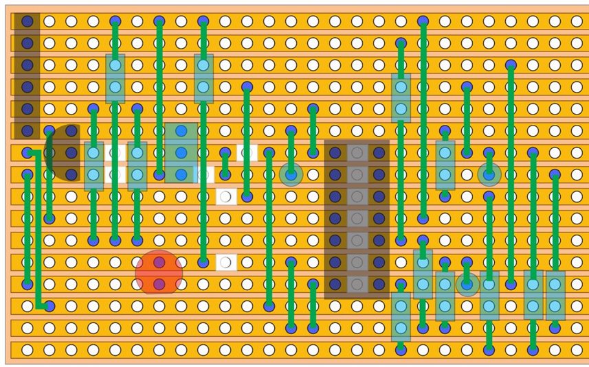
Here is a dusty old strip board sound synthesizer project which I plan to resurrect on a PCB:
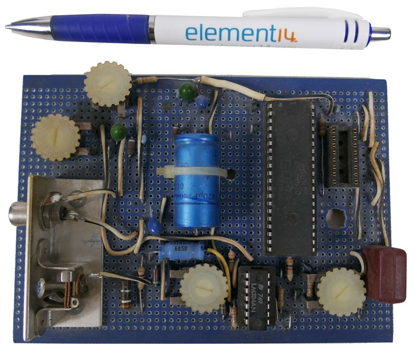
It works well for through-hole components and wire-wrap sockets. My first element 14 project (The Henrietta Project) was wired using a combination of strip-board and wire-wrap.

Wire-Wrap
Once in the work force I discovered wire-wrap and how productive it could be. This prompted me to invest in an electric wire-wrap gun, which is sill going strong. I even made a circuit to automatically limit the number of wraps, which further enhanced the machine (the circuit was made on strip board).
Here is a demo of how fast 3 LEDs can be wired up using wire-wrap:
Milling copper-clad board
There was a time when I wanted a CNC "engraver" to mill out circuits on copper clad fiberglass boards. However, before I could afford to buy one, SMT components became too small to make milling copper a practical solution.
An explanation of this method is explained here:
https://www.youtube.com/watch?v=ibZcQLIbets&ab_channel=ThomasSanladerer
From this video you can get some idea of how much work it is to mill out a decent circuit, which is a significant drawback to this method.
Traces can also be cut into copper-clad FR4 manually, and this technique is used quite a bit in prototyping RF circuits, but it never appealed to me. It just seemed like a lot of work to end up with a very ugly circuit board, especially if there are a lot of traces to cut and route.
Home etched PCBs
I also toyed with the idea of etching my own PCBs and did a lot of research on how to best apply etching masks with the least cost. However, before I actually pulled the trigger to buy all the chemicals, the price of manufactured PCBs came down to the point that they were much more attractive than dealing with storing, using and disposing of nasty chemicals.
An explanation of one method to perform home etching is shown here:
https://www.youtube.com/watch?v=cVhSCEPINpM&ab_channel=GarethBurrows
If you want a more professional board, you need a few more steps:
https://www.youtube.com/watch?v=IfhOYhjXLDg&ab_channel=MaxELECTRONICS
PCBs
For me, using PCBs is all about productivity - I want to complete my designs faster with fewer errors.
Although I use most of the above prototyping methods, I now do almost all of my prototyping on PCBs. I find it is far easier and faster to troubleshoot and fix PCB prototypes than any equivalent breadboard, proto-board or wire-wrap board, especially if I am going to make a PCB of the working circuit in the end anyway, and the cost ($0.50/card) is so low there is often no point in using other methods. And the result is a far better looking board. So far I have made at least 51 PCBs for element14 projects, and I can't remember any that didn't work on the first spin, although one or two didn't work perfectly. When I first started designing PCBs, there was no CAD, I had to build a light table so I could lay out the tracks with translucent colored tape. It was too expensive and I was too poor to make many prototypes this way, but I did made a few. I still have the first hobby PCB I ever designed: Rapid-fire joystick accessory.
Because PCBs are now my go-to prototyping method I will spend a bit more space describing how I do it.
CAD
I became a manger as CAD systems started to become available and consequently I have evaluated all major CAD systems 5 times in my career and I have used at least 7 CAD systems beyond simple evaluation activity. I eventually purchased CadSoft Eagle for my hobby activities, for a lot of reasons, but just to list a few:
- For my workflow, with the same person doing schematic capture and PCB layout, Eagle is far more productive than other CAD software. This is a big deal for me.
- I really like to have one screen showing the schematic and another screen showing the layout and have forward and backward annotation occur between screens in real time.
- At the time the price/performance ratio was much better than any other decent CAD package (the free version was extremely useful).
- There are some inexcusable idiosyncrasies with some other big name CAD systems that have cost board spins at every company I've worked at. Eagle does not have their main fatal flaw.
I am not at all keen on the licensing schemes employed by main stream CAD companies. I have not upgraded Eagle since AutoCad bought it and altered the licensing methods.
CAD Libraries save time when parts get reused since it takes time to enter component information, so it speeds up project when you use parts already in the library and since it also speeds up projects when using parts that are in stock, it makes sense to add stock components to the library.
I not only put components in the library, I also put whole modules, such as MCU modules like Arduino MKR or Raspberry Pi Pico or Arduino Pro Micro or HC05 Bluetooth modules. I also have header patterns for popular interfaces like Arduino Shields, TI Launchpads, Raspberry Pi Hats, Beaglebone Capes, Adafruit Feathers, etc. My list of display modules is also growing.
In fact all my previous designs or sections of them can be cut and pasted into new projects, saving a lot of time. The same philosophy carries through to the documentation I need to get the wiring correct. I can re-use old spreadsheets that detail interconnections, I just tweak them as needed.
Component stock - standardized
As alluded to above, it pays to keep a standard set of components in stock because it speeds up both design and build. I stock and use 0805 components wherever possible to keep stock at a reasonable cost and efficiently managed.
Resistors
For surface mount technology I have standardized on the E12 series of values to minimize the number of resistors that I need to stock. The E12 series has 12 values per decade where values are approximately evenly spaced on a logarithmic scale. I have 6 decades from 1 ohm to 10 MOhm which ends up to be 72 values. These are stored in a matrix of slots with the decade on one axis and the log value on the other axis.
Component kitting
When starting a build, I gather all the unusual parts into a project box so I don't have to go searching for parts during a build. Common components like resistors are organized separately in a custom dispenser system (shown above) so I can find the correct value with minimal effort.
Soldering, wet sponge and fume extraction setup
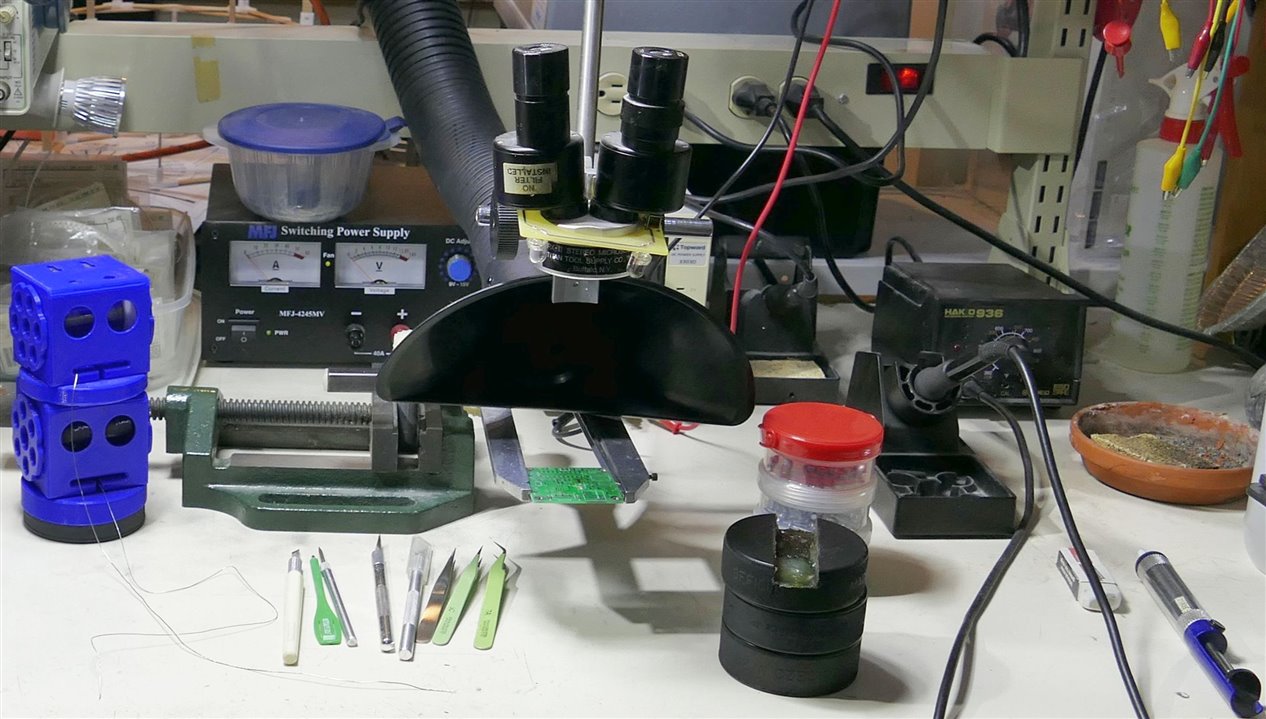
This image shows that the stereo microscope is in a fixed position but it allows the work to be positioned freely below it. The arrangement provides ample room to work the soldering iron while seeing details of the work.
Order of soldering - typically the smallest components are soldered first because the larger components can obstruct access to the smaller ones.
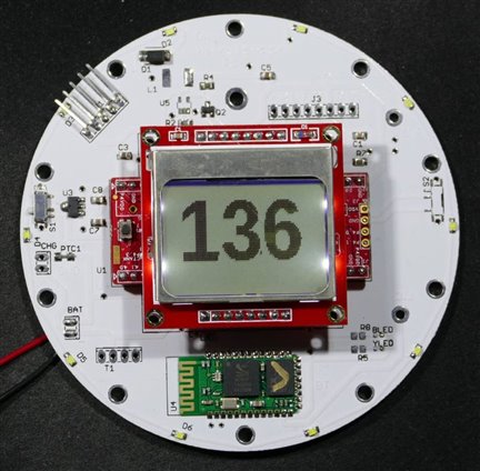
A Typical PCB (Heart Reactor) is shown here - it has an MCU module, a display, communications, sensors and controls. The same project included a Crown Tools system to record helmet impacts. It also has MCU, display, sensors, Bluetooth, and wireless charging in a 3D printed chassis.
Mechanical
Prototyping generally includes mechanical aspects of electronics, whether it is an electro-mechanical device or simply an enclosure. I won't dwell on mechanical prototyping since it is a large subject involving expensive tools and machines like milling machines, lathes, breaks, laser cutters and a host of others. Even the raw materials used, such as metal blocks, sheet metal, wood and plastic can be very expensive. Commercial plastic or metal project boxes are often used to minimize the cost of expensive tooling.
I want to briefly discuss 3D printing since it can replace many mechanical prototyping methods and is now an integral aspect of my electronic prototyping work. In some cases it replaces the PCB.
I follow a standard process - design a part with a CAD system (123D Design) and generate .stl files to 3D print the part. The CAD process uses a multi-window approach. One screen is the running the CAD software while the other screen runs many auxiliary programs, such as:
- several calculators and a spreadsheet to calculate dimensions
- datasheet viewers to obtain dimension of parts
- a slicing program to generate 3D printer files
- a browser to find related information
In addition to software I have a several rulers, protractors and a digital caliper to measure parts and circuits that need to fit in or attach to the package. I also have fairly high powered magnifiers to examine small details of components.
Finished devices often need labels, which can be either 3D printed or printed by a label machine.
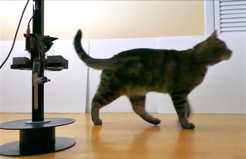
One reason why I am mentioning a mechanical prototyping process in a discussion of electronics prototyping is that it can replace the PCB in electronic systems, especially when they need to have components mounted at odd angles in a 3 dimensional geometry. I used exactly this method in my Snoop Cat project, where electronic components were mounted in 3D printed structures and used wire-wrap interconnections. Eventually low-cost printers will be able to print the interconnections as well as the 3D structure.
The Snoop Cat project is an example where 3D printing is integral to the electronics, taking the place of interconnection PCBs. (It also uses wire-wrap inter-module connections)
I have successfully used most of these techniques in projects on element14, so they are all still useful and appropriate in different situations.
Discussion
I hope this blog has provided some insight into how my prototyping methods have evolved.
It has been an interesting exercise to review prototyping techniques. In the future, techniques and methods and tools will continue to evolve. One way for me might be if I acquire a Voltera One which can print PCB prototypes without involving external fab shops. Beyond that it will likely be some time before machines that can print full 3D electronic systems become cheap enough for hobbyists to access. But then, I never thought I would be buying PCBs for $0.50 each.
Relevant links:

Top Comments