Here are the previous blogs in this series:
Prototyping with FPGAs - Part 1 - Basics
Prototyping with FPGAs - Part 2 - Combinational Logic with Xilinx ISE on Spartan 6 FPGA
Part 2 explains how to program a Spartan 6 FPGA using the Xilinx ISE, in this blog, I'll be explaining how to program a Cyclone IV FPGA using Quartus Prime software.
The design flow is the same for all FPGAs as mentioned in Part 2, just different names but the underlying algorithm is not much different.
I'm going to use the DE0-Nano Development board in this project. One good thing about using DE0 Nano is that it has a lot of supporting tools such as the Terasic System Builder which creates a project with all required files such as the master constraints and timing constraints files.
This blog will take you through a design of an 8-bit counter with a frequency divider in Verilog HDL to convert 50MHz into 1Hz clock frequency and implementation on Cyclone IV FPGA.
What is Sequential logic?
Sequential logic is a type of logic circuit whose output depends not only on the present value of its input signals but on the sequence of past inputs that means it has memory elements.
Design for FPGA:
Open Terasic System Builder and do the following steps:
| {gallery} SB |
|---|
Open Terasic DE0-Nano System Builder and select required system components |
Save the generated files in project Directory |
Generated Files |
Now the required files such as the Quartus Prime Project File (QPF File), Quartus Prime Settings File (QSF File), and Synopsys Design Constraints File (SDC File) are generated in the project location.
Getting started with Quartus Prime:
| {gallery} QP |
|---|
Open the project from Quartus Prime |
IMAGE TITLE: THEN IMAGE DESCRIPTION |
Write the program for frequency divider and Counter |
Add other files which are required for the design |
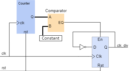
I'm going to implement something very similar to this but in a different modeling style.
Why frequency divider?
The output clock frequency of the onboard clock is usually in the range of MHz to support fast computations, but in order to realize the counting, the clock speed should be slow enough to be visible to our naked eye.
Thus we divide the frequency to get lower clock frequencies.
Design of a frequency divider:
Verilog code:
The constant value here is 25 Million (where onboard clock = 50MHz), which signifies 0.5 seconds ON and 0.5 seconds OFF time of the 1Hz clock.
Design of 8-bit counter:
As you can see, the design is pretty simple, a series of flip-flops that store one bit of data and a full adder as discussed in Part 2 of the blog series.
Verilog Code:
Here the module Counter has the 50MHz onboard clock as the input thus we divide and reduce it to a 1Hz clock by feeding it to the Frequency divider module by instantiating it (see line 8).
Complete Design (Expected):
Synthesized:
Now it's time to write the constraints file for design implementation.
Constraints file:
SDC File:
As we have Synthesis, Implementation and bitstream generation in ISE, it's called as Analysis & Synthesis, Fitter and then Assembler in Quartus Prime. Apparently, all do the same job.
Hit compile!
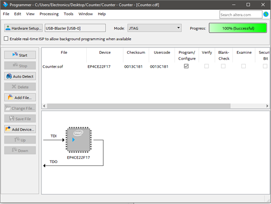
Then Open the Programmer and then click on Start.
Then it'll show the successful message once the device is programmed.
As the 8-bits of count is tied to the onboard LEDs (check constraints file). Thus, the output can be viewed onboard!
Output:
Thanks for reading!


