element14 Community
element14 Community
    Register Log In
  • Site
  • Search
  • Log In Register
  • About Us
  • Community Hub
    Community Hub
    • What's New on element14
    • Feedback and Support
    • Benefits of Membership
    • Personal Blogs
    • Members Area
    • Achievement Levels
  • Learn
    Learn
    • Ask an Expert
    • eBooks
    • element14 presents
    • Learning Center
    • Tech Spotlight
    • STEM Academy
    • Webinars, Training and Events
    • Learning Groups
  • Technologies
    Technologies
    • 3D Printing
    • FPGA
    • Industrial Automation
    • Internet of Things
    • Power & Energy
    • Sensors
    • Technology Groups
  • Challenges & Projects
    Challenges & Projects
    • Design Challenges
    • element14 presents Projects
    • Project14
    • Arduino Projects
    • Raspberry Pi Projects
    • Project Groups
  • Products
    Products
    • Arduino
    • Avnet Boards Community
    • Dev Tools
    • Manufacturers
    • Multicomp Pro
    • Product Groups
    • Raspberry Pi
    • RoadTests & Reviews
  • Store
    Store
    • Visit Your Store
    • Choose another store...
      • Europe
      •  Austria (German)
      •  Belgium (Dutch, French)
      •  Bulgaria (Bulgarian)
      •  Czech Republic (Czech)
      •  Denmark (Danish)
      •  Estonia (Estonian)
      •  Finland (Finnish)
      •  France (French)
      •  Germany (German)
      •  Hungary (Hungarian)
      •  Ireland
      •  Israel
      •  Italy (Italian)
      •  Latvia (Latvian)
      •  
      •  Lithuania (Lithuanian)
      •  Netherlands (Dutch)
      •  Norway (Norwegian)
      •  Poland (Polish)
      •  Portugal (Portuguese)
      •  Romania (Romanian)
      •  Russia (Russian)
      •  Slovakia (Slovak)
      •  Slovenia (Slovenian)
      •  Spain (Spanish)
      •  Sweden (Swedish)
      •  Switzerland(German, French)
      •  Turkey (Turkish)
      •  United Kingdom
      • Asia Pacific
      •  Australia
      •  China
      •  Hong Kong
      •  India
      •  Korea (Korean)
      •  Malaysia
      •  New Zealand
      •  Philippines
      •  Singapore
      •  Taiwan
      •  Thailand (Thai)
      • Americas
      •  Brazil (Portuguese)
      •  Canada
      •  Mexico (Spanish)
      •  United States
      Can't find the country/region you're looking for? Visit our export site or find a local distributor.
  • Translate
  • Profile
  • Settings
Test Instrumentation
  • Challenges & Projects
  • Project14
  • Test Instrumentation
  • More
  • Cancel
Test Instrumentation
Blog "No lies" IR Thermometer - part II
  • Blog
  • Forum
  • Documents
  • Events
  • Polls
  • Files
  • Members
  • Mentions
  • Sub-Groups
  • Tags
  • More
  • Cancel
  • New
Join Test Instrumentation to participate - click to join for free!
  • Share
  • More
  • Cancel
Group Actions
  • Group RSS
  • More
  • Cancel
Engagement
  • Author Author: koudelad
  • Date Created: 23 Sep 2018 8:26 PM Date Created
  • Views 2073 views
  • Likes 11 likes
  • Comments 8 comments
  • target 3001
  • ir_thermometer
  • psoc 4
  • diytestinstruch
Related
Recommended

"No lies" IR Thermometer - part II

koudelad
koudelad
23 Sep 2018
image

Test Instrumentation

Enter Your Electronics & Design Project for a chance to win a Grand Prize for Originality, a Tool Set, and a $100 Shopping Cart!

Back to The Project14 homepage image

Project14 Home
Monthly Themes
Monthly Theme Poll


Blog posts:

"No lies" IR Thermometer - part I

This is part 2

"No lies" IR Thermometer - part III

"No lies" IR Thermometer - part IV


IR thermometer v1 – the hardware

In my previous blog post I described my motivation to build my own body IR thermometer, included a few sentences about the principles and showed 2 prototypes using a ready-made development kit and a breadboard with PSoC 5LP and PSoC 4 devices. I also mentioned, that I wanted to create my first professionally made PCB.


As written before, my approach is to do incremental development, one step at a time. You will definitely see images of electronics made by an amateur. However, my goal is to learn at least a small bit of something new every time I am doing something, so feel free to comment what can I make better next time.


The design software

The first step to create a PCB is usually creating schematics. Why usually? I have a friend that has a good memory and a sense of routing signals, so he usually draws PCBs with up to ca. 300 components (yes, three hundred) in his design software straight away.


I am a fan of more planning (drawing schematics) and only after that, placing the components and drawing tracks. About 10 years ago, almost every amateur I met (physically or on the internet) used EAGLE. I never really got used to the controls, so I tried about 10 design programs and then found Target 3001! The fun part is, I tried EAGLE, KiCAD and some software packages offered by component distributors and ended up with Target 3001! again. I don’t want to make any advertisement and I have no interest in doing so, but I like the software for two things. First, it gets the job done quickly, the controls are quite intuitive for me. Second, it is being developed almost three decades by a family company. If you write them an email and ask for support, it is not unusual you get an answer from the founder or his son. Pretty rare these days.
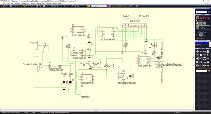
 

The schematics

It won’t be surprising how I started drawing. I found the schematics of the PSoCRegistered 4 CY8CKIT-049 4200 Prototyping Kit, removed what wasn’t necessary and added all the components from the breadboard.


Just a few notes about the design:


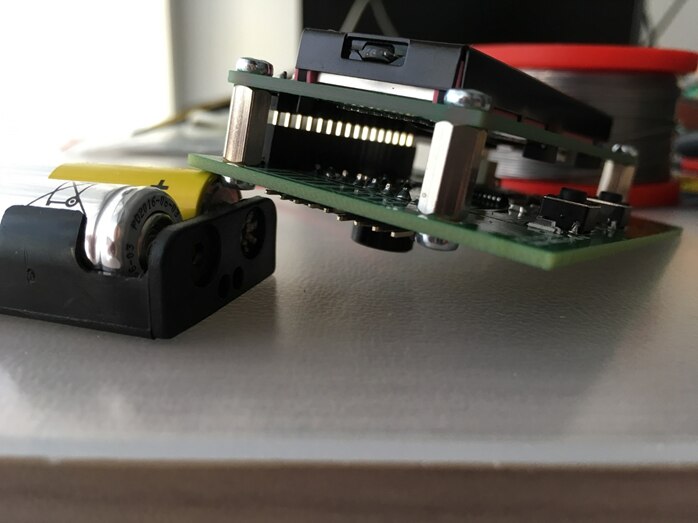
J1 is a power connector and the idea is to power the device directly by 2 AA or AAA alkaline batteries.


J5 is a connector intended for UART. I might find it useful in the future, but it is not implemented at the moment.


There are two push buttons and one LED. The LED has no function and only one of the buttons starts the measurement. The other button has no function. Both buttons have unpopulated pin header in parallel with them. My idea was to embed the device into a box, but leave the possibility to control the thermometer without the box, too.


Here comes the full schematics. I know, it is kind of chaotic.
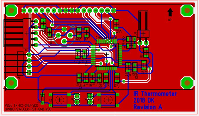
image


PCB

And the PCB I drew based on the schematics. My first PCB sent to a PCB manufacturer ever image

image


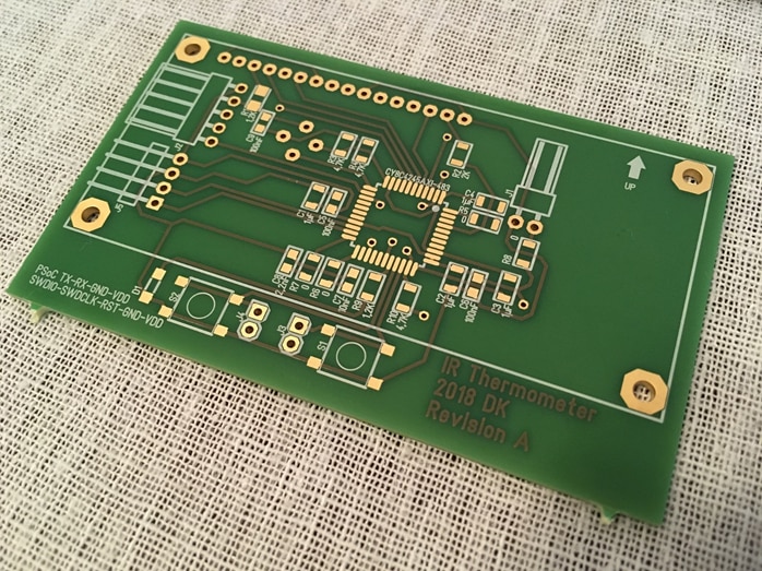
I ordered the PCB at a smaller Czech company to show some support to local companies. My friend helped me to prepare the data (especially for the pool service, which makes the PCB cheaper). I thought exporting should be easy, but it is worth asking the manufacturer about formats etc. to avoid additional costs of manual adjustments at the manufacturing facility.


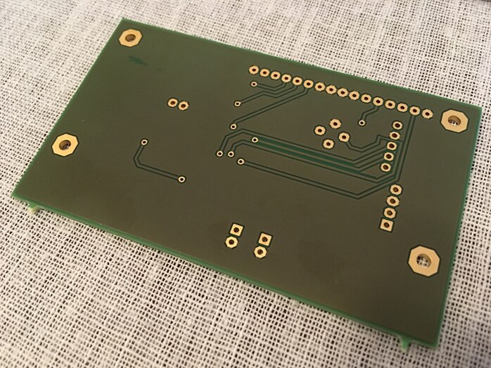
One week passed and this is what I got:

image

image


I also knew that I wouldn’t be able to solder the chip with my current soldering iron. So, this was a perfect excuse to buy a new one, with a finer handle and a tip. Plus, better solder and flux. I have seen many videos on YouTube and they have one thing in common. Professionals looking for a professional outcome use a good quality soldering iron, solder and flux.


By the way, have you seen this series of soldering in avionics industry? Must see for everyone looking for a professional soldering result. https://www.youtube.com/watch?v=0SnOW2VdCTI . I don’t say all should do it this way, but it is worth knowing all the steps.


Here is my soldering. On the left is the thermometer PCB, on the right is a simple practice board bought for a few Euros. I highly recommend practicing after longer periods of not soldering.


image

image

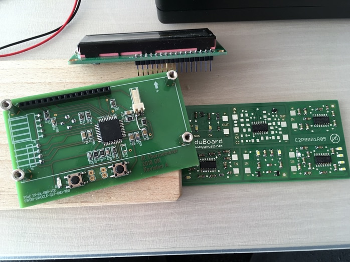
As you can see, there is a jumper wire between the power connector and ground of the remaining board. I made an error concatenating signals, which was discovered after assembly image


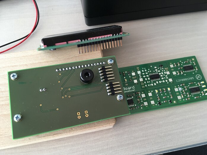
And last, finalized assembly of version 1.

image

image


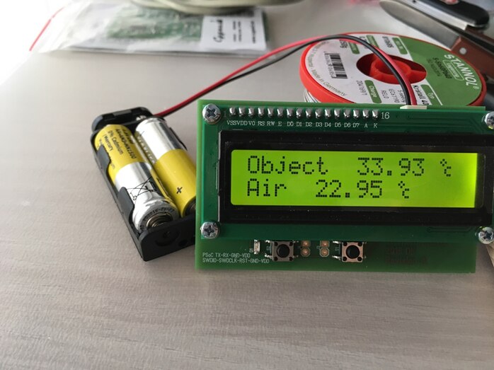
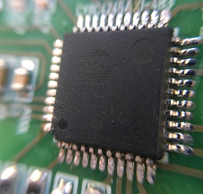
Did it work on the first power up? No – it took me a week to figure out I rotated the chip by 180 degrees. The chip has two circular markings at the edges and when I soldered the chip, I haven’t noticed it. The smaller one is the correct (and mentioned in the datasheet). Fun fact: according to the datasheet is the chip label irrelevant to the chip orientation.

Fortunately, I was able to remove the chip using a common hot air gun (not for soldering) and solder it again.

image


Did it work on the second power up? No – it took me another week to find a missing ground connection.


My takeaways

  • If the design software features a design rule check, use it. If I had used it properly, I wouldn’t have soldered the jumper wire between two different ground signals.
  • Use one size of components if possible. I mixed 1206 and 0805 resistors and capacitors. The less sizes, the better to maintain stock supplies.
  • Do not play with mirroring the components on the PCB. I mirrored two connectors (serial port and programming header) and then had to solder them from the other side to keep the layout as printed on solder mask. I was fortunate with this 2,54 mm header, but other connector types would mean a useless PCB.
  • Have a proper lightning and make sure all components are placed on the right places.


TO BE CONTINUED


David

  • Sign in to reply

Top Comments

  • fmilburn
    fmilburn over 6 years ago +5
    Hi David, that is fairly advanced for your first PCB and is looking quite nice. Frank
  • koudelad
    koudelad over 6 years ago +5
    Thanks to all of you for the kind words. Well, it is a first professionally manufactured PCB and the first made PCB after 15 years. I used the same program before to draw one or two PCBs when I was about…
  • shabaz
    shabaz over 6 years ago +4
    Hi David, That's really impressive. I can't recall my first PCB but I'm sure it must have been really bad. Also it is interesting to see the Melexis device being used - they make nice sensors, but they…
  • Marvian
    Marvian over 1 year ago

    Hi David, I am new to PSOC5 and I love this project and try to build it but I could not to read the IR, project files the google drive link does not work and I appreciate for sharing  the files.

    • Cancel
    • Vote Up 0 Vote Down
    • Sign in to reply
    • More
    • Cancel
  • three-phase
    three-phase over 6 years ago

    Great update on your project.


    Kind regards.

    • Cancel
    • Vote Up +3 Vote Down
    • Sign in to reply
    • More
    • Cancel
  • shabaz
    shabaz over 6 years ago in reply to 14rhb

    Ohh, etch-resist stress cracks : ) .. I tried the letraset stuff and crepe reels.. amazed that anything got done with stuff like this image I still have a photocopy of some layout I tried like that somewhere.. it's really bad : )

    • Cancel
    • Vote Up +3 Vote Down
    • Sign in to reply
    • More
    • Cancel
  • koudelad
    koudelad over 6 years ago

    Thanks to all of you for the kind words.


    Well, it is a first professionally manufactured PCB and the first made PCB after 15 years.


    I used the same program before to draw one or two PCBs when I was about 15. I only used through-hole components and the layout looked exactly the same as schematics. The PCB also had many faults... for example the default pad sizes... they were so small I drilled them away during drilling the holes. And I was trying to drill 0,8 or 0,6 mm holes with a hobby 5-10$ drill (the ones with a DC motor without any gears).

    My method was to print on a special foil for ink printers (at home, of course) and than attach the printed side to the photo-resistive copper. I used UV light or plain 500 W light to expose and NaOH to wash away the exposed film. Then all went to FeCl3.

    I also accidentally mirrored the printed PCB image a few times, so I had a few beautiful, but completely useless boards image


    However, even before that, I tried scratching a plain copper layer and also another PCB by drawing with a special pen and etching in FeCl3. Both was terrible. And the worst part - I had no idea that the copper needs some finish to avoid corrosion.


    I don't have any of those PCBs, it was an interesting experience making them, but quite painful, because I didn't know anyone else making his own PCBs. There were so many unsuccessful attempts, but I had the time and learned a lot.


    David

    • Cancel
    • Vote Up +5 Vote Down
    • Sign in to reply
    • More
    • Cancel
  • 14rhb
    14rhb over 6 years ago in reply to shabaz

    Hi Shabaz,


    I can only too well recall my first homebrew PCB although not the functionality of it. I drew it out with a PCB pen and transfers - it looked good. But to save on etcher I decided to chop some of the excess board away and in doing so added far too may fine lines to the etch resist. I only noticed post-etch image


    Rod

    • Cancel
    • Vote Up +3 Vote Down
    • Sign in to reply
    • More
    • Cancel
>
element14 Community

element14 is the first online community specifically for engineers. Connect with your peers and get expert answers to your questions.

  • Members
  • Learn
  • Technologies
  • Challenges & Projects
  • Products
  • Store
  • About Us
  • Feedback & Support
  • FAQs
  • Terms of Use
  • Privacy Policy
  • Legal and Copyright Notices
  • Sitemap
  • Cookies

An Avnet Company © 2025 Premier Farnell Limited. All Rights Reserved.

Premier Farnell Ltd, registered in England and Wales (no 00876412), registered office: Farnell House, Forge Lane, Leeds LS12 2NE.

ICP 备案号 10220084.

Follow element14

  • X
  • Facebook
  • linkedin
  • YouTube