element14 Community
element14 Community
    Register Log In
  • Site
  • Search
  • Log In Register
  • Community Hub
    Community Hub
    • What's New on element14
    • Feedback and Support
    • Benefits of Membership
    • Personal Blogs
    • Members Area
    • Achievement Levels
  • Learn
    Learn
    • Ask an Expert
    • eBooks
    • element14 presents
    • Learning Center
    • Tech Spotlight
    • STEM Academy
    • Webinars, Training and Events
    • Learning Groups
  • Technologies
    Technologies
    • 3D Printing
    • FPGA
    • Industrial Automation
    • Internet of Things
    • Power & Energy
    • Sensors
    • Technology Groups
  • Challenges & Projects
    Challenges & Projects
    • Design Challenges
    • element14 presents Projects
    • Project14
    • Arduino Projects
    • Raspberry Pi Projects
    • Project Groups
  • Products
    Products
    • Arduino
    • Avnet & Tria Boards Community
    • Dev Tools
    • Manufacturers
    • Multicomp Pro
    • Product Groups
    • Raspberry Pi
    • RoadTests & Reviews
  • About Us
  • Store
    Store
    • Visit Your Store
    • Choose another store...
      • Europe
      •  Austria (German)
      •  Belgium (Dutch, French)
      •  Bulgaria (Bulgarian)
      •  Czech Republic (Czech)
      •  Denmark (Danish)
      •  Estonia (Estonian)
      •  Finland (Finnish)
      •  France (French)
      •  Germany (German)
      •  Hungary (Hungarian)
      •  Ireland
      •  Israel
      •  Italy (Italian)
      •  Latvia (Latvian)
      •  
      •  Lithuania (Lithuanian)
      •  Netherlands (Dutch)
      •  Norway (Norwegian)
      •  Poland (Polish)
      •  Portugal (Portuguese)
      •  Romania (Romanian)
      •  Russia (Russian)
      •  Slovakia (Slovak)
      •  Slovenia (Slovenian)
      •  Spain (Spanish)
      •  Sweden (Swedish)
      •  Switzerland(German, French)
      •  Turkey (Turkish)
      •  United Kingdom
      • Asia Pacific
      •  Australia
      •  China
      •  Hong Kong
      •  India
      •  Korea (Korean)
      •  Malaysia
      •  New Zealand
      •  Philippines
      •  Singapore
      •  Taiwan
      •  Thailand (Thai)
      • Americas
      •  Brazil (Portuguese)
      •  Canada
      •  Mexico (Spanish)
      •  United States
      Can't find the country/region you're looking for? Visit our export site or find a local distributor.
  • Translate
  • Profile
  • Settings
Essentials
  • Learn
  • Learning Center
  • Essentials
  • More
  • Cancel
Essentials
Forum Experimenting with Op Amps: active full-wave rectifier
  • Forum
  • Documents
  • Polls
  • Files
  • Members
  • Mentions
  • Sub-Groups
  • Tags
  • More
  • Cancel
  • New
Join Essentials to participate - click to join for free!
Actions
  • Share
  • More
  • Cancel
Forum Thread Details
  • Replies 21 replies
  • Subscribers 1015 subscribers
  • Views 8648 views
  • Users 0 members are here
  • opamp
  • analogue
  • analog
Related

Experimenting with Op Amps: active full-wave rectifier

Jan Cumps
Jan Cumps over 2 years ago

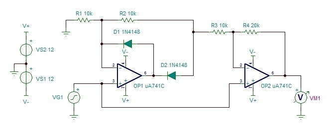
The Art Of Electronics features a set of practical op-amp circuits. They have several full-wave rectifiers. I'm trying the simplest one. You don't need fancy devices. A pair of 741s will do.

The circuit:

image
image source: my copy of the book. fair use.

Looking at the node where the arrow points to:

  • for positive values, the first op-amp is an inverting buffer.
  • for negative values, the op-amp output has a  0.6V dc bias, the right side of  the feedback resistor will be at 0 V (ground). 
    hint: the 0.6 V output is generated by the op-amp to drive the inverting input to the same value as the + input (ground), effectively clamping the output to 1 diode drop above ground.

image

Looking at the second op-amp:

  • it is an op-amp with a summing node. Two signals at the inverting input are summed and inverted. The amplification factor is defined by the input resistor and the feedback resistor.
  • for the input signal, the amplification = -1 * R/R = -1 (the input resistance equals the feedback resistance, resulting in the -1 amplification factor, doubling and inverting the signal)
  • for the signal coming from op-amp 1, the amplification = -1 * R / (R/2) = -2 (the input resistance is half the feedback resistance, resulting in the -2 amplification factor)
  • it is an inverting amplifier for the input. Both positive and negative signals are amplified by -1.
  • for the signal coming from the first op-amp, it acts as a -2 amplifier.
  • for positive inputs, this results in  Vin * -1 + Vin * -1 * -2 = -Vin + 2Vin = Vin ->  result: Vin, positive Vin comes out as positive Vin (see comment)
  • for negative inputs, this results in Vin * -1 (making Vin positive)  + Vin * 0 * -1 -> result -Vin: negative Vin comes out as positive Vin

image

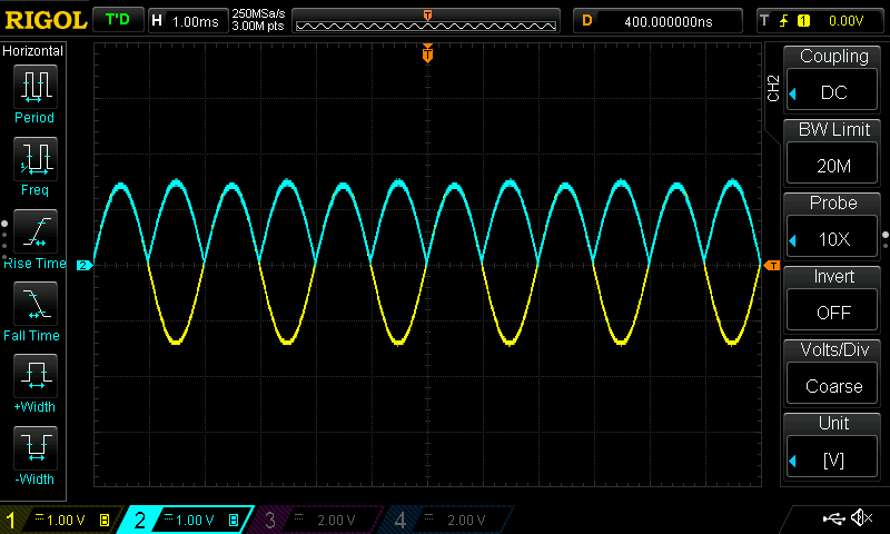
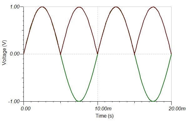
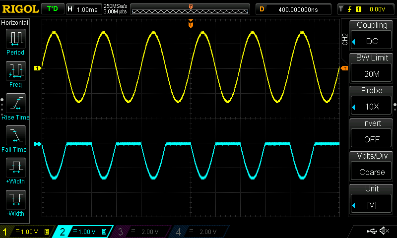
Here is the result: The blue line is the output. Underneath it, you see the input. The output overlaps the input for the positive part. It inverses the negative part. No diode drop.

image

  • Sign in to reply
  • Cancel

Top Replies

  • Jan Cumps
    Jan Cumps over 2 years ago +5
    If you are puzzled by the circuit, there is a way to understand it: Build the first op-amp circuit and feed a sinus into it. Try it with and without the vertical diode. Try to understand why it is…
  • anniel747
    anniel747 over 2 years ago in reply to Jan Cumps +4
    Deleted
  • javagoza
    javagoza over 2 years ago in reply to anniel747 +4
  • Jan Cumps
    Jan Cumps over 2 years ago in reply to michaelkellett
    michaelkellett said:
    Just for fun try scoping the output of A1 and high frequencies

    40 kHz:

    image

    • Cancel
    • Vote Up +1 Vote Down
    • Sign in to reply
    • Cancel
  • Jan Cumps
    Jan Cumps over 2 years ago in reply to Jan Cumps
    michaelkellett said:
    Just for fun try scoping the output of A1 and [...] with a low amplitude signal

    500 Hz, 70 mVpp. I had to turn on averaging because the whole scope screen was smeared with noise:

    image

    (in this capture, channel 3 is in different vertical range than the 3 other channels)

    • Cancel
    • Vote Up +1 Vote Down
    • Sign in to reply
    • Cancel
  • michaelkellett
    michaelkellett over 2 years ago in reply to Jan Cumps

    The first op amp in this design has a hard time because it has to swing the diode drop and more in a small fraction of a cycle time. The smaller the signal the worse the effect.

    Some of the true RMS chips have a similar problem, good frequency response with large signals but much less good with small. I can remember struggling to get the required accuracy over amplitude and frequency in a meter design for BT in about 1978.

    MK

    • Cancel
    • Vote Up +2 Vote Down
    • Sign in to reply
    • Cancel
  • Jan Cumps
    Jan Cumps over 2 years ago in reply to Jan Cumps

    Measurements when the input is  +3.23 V dc.

    image

    You can see here that for positive inputs, the horizontal diode does not conduct, and the 10K feedback resistor comes into play.
    The 3.24 V input is inverted, and its inverse is passed to circuit 2.

    The second op-amp, the inverting summing amp, has different gain for both inputs. The gain = -(Rfeedback / Rin)
    For the original +3.23 V input, with gain -1 (-10K/10K), we'd get -3.23 V output.
    For the -3.23 V V signal coming from the first circuit, with gain -2 (-10K/5K), we'd get +6.46V output
    Summed up, this is +3.23 V output.

    • Cancel
    • Vote Up 0 Vote Down
    • Sign in to reply
    • Cancel
  • Jan Cumps
    Jan Cumps over 2 years ago in reply to michaelkellett
    michaelkellett said:
    The first op amp in this design has a hard time because it has to swing the diode drop and more in a small fraction of a cycle time.

    The struggle is visible on this 11 kHz capture (input: 2Vpp)

    image

    • Cancel
    • Vote Up +3 Vote Down
    • Sign in to reply
    • Cancel
  • DAB
    DAB over 2 years ago

    Very cool experiment Jan.

    • Cancel
    • Vote Up +1 Vote Down
    • Sign in to reply
    • Cancel
  • Jan Cumps
    Jan Cumps over 2 years ago in reply to Jan Cumps

    (I burned half the weekend reading that book)

    • Cancel
    • Vote Up 0 Vote Down
    • Sign in to reply
    • Cancel
  • flyingbean
    flyingbean over 2 years ago
    Jan Cumps said:
    for positive inputs, this results in  Vin * -1 + Vin * -2 = Vin ->  result: Vin, positive Vin comes out as Vin

    I think for positive input, Vin*(-1) +(-1)*Vin *(-2) = Vin -> result: Vin

    • Cancel
    • Vote Up +1 Vote Down
    • Sign in to reply
    • Cancel
  • jc2048
    jc2048 over 2 years ago

    This is another one you see sometimes. I got this from Analog Signal Processing by R Pallas-Areny and J G Webster. One less resistor and high impedance input. Works ok in a simulator.

    image

    image
    Has same problems as all of these when the input transitions through zero and it switches between the two modes of operation.

    If you want to practice your circuit-analysing skills (in-head simulation), there is a potential problem with it that makes it less flexible than the one you showed.

    • Cancel
    • Vote Up +3 Vote Down
    • Sign in to reply
    • Cancel
  • anniel747
    anniel747 over 2 years ago in reply to Jan Cumps
    [deleted]
    • Cancel
    • Vote Up +4 Vote Down
    • Sign in to reply
    • Cancel
<>
element14 Community

element14 is the first online community specifically for engineers. Connect with your peers and get expert answers to your questions.

  • Members
  • Learn
  • Technologies
  • Challenges & Projects
  • Products
  • Store
  • About Us
  • Feedback & Support
  • FAQs
  • Terms of Use
  • Privacy Policy
  • Legal and Copyright Notices
  • Sitemap
  • Cookies

An Avnet Company © 2025 Premier Farnell Limited. All Rights Reserved.

Premier Farnell Ltd, registered in England and Wales (no 00876412), registered office: Farnell House, Forge Lane, Leeds LS12 2NE.

ICP 备案号 10220084.

Follow element14

  • X
  • Facebook
  • linkedin
  • YouTube