element14 Community
element14 Community
    Register Log In
  • Site
  • Search
  • Log In Register
  • About Us
  • Community Hub
    Community Hub
    • What's New on element14
    • Feedback and Support
    • Benefits of Membership
    • Personal Blogs
    • Members Area
    • Achievement Levels
  • Learn
    Learn
    • Ask an Expert
    • eBooks
    • element14 presents
    • Learning Center
    • Tech Spotlight
    • STEM Academy
    • Webinars, Training and Events
    • Learning Groups
  • Technologies
    Technologies
    • 3D Printing
    • FPGA
    • Industrial Automation
    • Internet of Things
    • Power & Energy
    • Sensors
    • Technology Groups
  • Challenges & Projects
    Challenges & Projects
    • Design Challenges
    • element14 presents Projects
    • Project14
    • Arduino Projects
    • Raspberry Pi Projects
    • Project Groups
  • Products
    Products
    • Arduino
    • Avnet Boards Community
    • Dev Tools
    • Manufacturers
    • Multicomp Pro
    • Product Groups
    • Raspberry Pi
    • RoadTests & Reviews
  • Store
    Store
    • Visit Your Store
    • Choose another store...
      • Europe
      •  Austria (German)
      •  Belgium (Dutch, French)
      •  Bulgaria (Bulgarian)
      •  Czech Republic (Czech)
      •  Denmark (Danish)
      •  Estonia (Estonian)
      •  Finland (Finnish)
      •  France (French)
      •  Germany (German)
      •  Hungary (Hungarian)
      •  Ireland
      •  Israel
      •  Italy (Italian)
      •  Latvia (Latvian)
      •  
      •  Lithuania (Lithuanian)
      •  Netherlands (Dutch)
      •  Norway (Norwegian)
      •  Poland (Polish)
      •  Portugal (Portuguese)
      •  Romania (Romanian)
      •  Russia (Russian)
      •  Slovakia (Slovak)
      •  Slovenia (Slovenian)
      •  Spain (Spanish)
      •  Sweden (Swedish)
      •  Switzerland(German, French)
      •  Turkey (Turkish)
      •  United Kingdom
      • Asia Pacific
      •  Australia
      •  China
      •  Hong Kong
      •  India
      •  Korea (Korean)
      •  Malaysia
      •  New Zealand
      •  Philippines
      •  Singapore
      •  Taiwan
      •  Thailand (Thai)
      • Americas
      •  Brazil (Portuguese)
      •  Canada
      •  Mexico (Spanish)
      •  United States
      Can't find the country/region you're looking for? Visit our export site or find a local distributor.
  • Translate
  • Profile
  • Settings
Community Hub
Community Hub
Member's Forum Testing a Mosfet and Schottky in-circuit; Bit more advice
  • Blog
  • Forum
  • Documents
  • Quiz
  • Events
  • Leaderboard
  • Polls
  • Files
  • Members
  • Mentions
  • Sub-Groups
  • Tags
  • More
  • Cancel
  • New
Join Community Hub to participate - click to join for free!
Actions
  • Share
  • More
  • Cancel
Forum Thread Details
  • State Suggested Answer
  • Replies 31 replies
  • Answers 27 answers
  • Subscribers 530 subscribers
  • Views 6505 views
  • Users 0 members are here
Related

Testing a Mosfet and Schottky in-circuit; Bit more advice

Andrew J
Andrew J over 6 years ago

I presume this is possible with power off, looking for resistance between drain and source?


I'm pretty sure I've killed it - resistance is 0.33Ohms between these two pins image  Out of circuit, on a good one, it is > 13MOhms.  Looking at my circuit, I've solder the Schottky Rectifier the wrong way around - cathode to ground imageimageimage  Pretty sure that won't have done the Mosfet any good, it was too hot to touch.  Can't believe I've been so stupid - by good luck, rather than management, the other Schottky I have in the circuit (not shown below) is the right way around.


Is there a way of testing the Schottky rectifier in-circuit - I've tried it and the DMM 'beeps' as it detects a normal junction; measures 0.159v and 0.579V depending upon orientation of test leads?  Just to clarify - in the schematic below you can see how the Schottky rectifier should be - however, as I say, it's actually reversed and I don't know if that might affect readings. So, with the COM lead to the cathode and test (red) lead to anode it reads 0.159v; with the COM lead to the anode and test (red) lead to cathode it reads 0.579V.  I can test one out of circuit and I get 0.157V and OL respectively.  I think that indicates it is ok but in circuit it isn't reading as OL: I have to remove it to swap it around in any case so would the advice be to chuck it and use a new one? 


I'm really hoping I can get it off with wick and an iron and without damaging the board; ditto the Mosfet. I really don't want to lump out for a rework station.


Is there likely to be damage to other components down stream?  Any tips for testing components without removing them from the circuit?


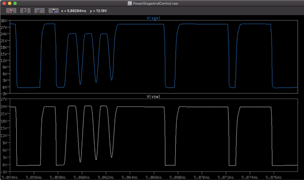
This is only part of the circuit but shows the relationship between the Mosfet and Schottky rectifier:


image


[silently screaming inside]

  • Sign in to reply
  • Cancel

Top Replies

  • jc2048
    jc2048 over 6 years ago +7 suggested
    Resistance reading in-circuit is difficult because of paths round through the power and through the ICs [via the protection circuits]. You'll tend to see initially low readings that move because you're…
  • jc2048
    jc2048 over 6 years ago in reply to jw0752 +6 suggested
    0.159V doesn't look too unreasonable for a test current of between 1mA and 10mA.
  • jc2048
    jc2048 over 6 years ago in reply to Andrew J +6 suggested
    It's good that you see something sensible on the Ith/RUN pin. At least it's doing something and not totally dead. Do you see voltage on the BOOST pin? Initially, the boost capacitor charges from the internal…
Parents
  • jc2048
    0 jc2048 over 6 years ago

    Resistance reading in-circuit is difficult because of paths round through the power and through the ICs [via the protection circuits]. You'll tend to see initially low readings that move because you're charging decoupling capacitors. I don't like doing it because of the possibility of damage to chips [a handheld meter is probably worse than a good bench meter in that respect], but then I tend to be very over-cautious.


    Commercially, you'd chuck the components and use new ones (the parts cost is much, much lower than the cost to you of a person messing around with parts that are suspect). Actually, you might well label the board carefully, put it to one side, and move to the next, unused prototype, unless there were good reasons for sticking with the same one.


    For a personal project it's different and you may want to experiment a bit. The MOSFET and Schottky are fairly robust. Just because you can't bear to touch it doesn't mean it is dead. The controller is working current mode, monitoring the current through the MOSFET with R2. With the back-to-front Schottky clamping the output, the controller would keep increasing the current through the MOSFET to try and get the voltage up but there would be some limit to that, so the part's dissipation wouldn't necessarily have been enough to destroy it.


    So you might try just reworking the Schottky [if the Schottky SMD package is the type with fold-under legs, they're easy to get off even with a standard soldering iron as you can lift one end at a time]. Are you able to substitute a bench supply for the power rail? If so, one approach might be to apply a very low voltage that was under the controllers's lock-out voltage and was safe for the following circuit and see if the MOSFET feeds that to the coil without there being any gate drive.


    The feedback arrangement is a bit odd [and, possibly, a bit dangerous]. If you lost the connection to R6 you'd lose the feedback and the converter would ramp up the voltage to try and compensate, so you want to be careful with that depending on where it comes from and what it's supposed to be doing.

    • Cancel
    • Vote Up +7 Vote Down
    • Sign in to reply
    • Verify Answer
    • Reject Answer
    • Cancel
  • Andrew J
    0 Andrew J over 6 years ago in reply to jc2048

    I wasn't sure how possible it was to test in-circuit and how skewed the result would be. 


    However, having taken both pieces of the board, the Schottky rectifier is reading 0.159Ohms and OL; a known good one is reading 0.157Ohms and OL.  I think that's ok and I put it back on the board in the correct orientation.


    The Mosfet is reading 0.33Ohms between drain and source (out of circuit).  A known good one is reading >34MOhms.  So I think the one I removed is dead.  In goes a new one and back to testing.

    • Cancel
    • Vote Up +5 Vote Down
    • Sign in to reply
    • Verify Answer
    • Reject Answer
    • Cancel
  • Andrew J
    0 Andrew J over 6 years ago in reply to Andrew J

    Well, on the plus side, I haven't refried the Mosfet!  On the other hand, something isn't working the way it should as it's not turning on - gate voltage is only 0.5V.  U1 is definitely turned on - the ith/run voltage is >1.9V; it's getting power to Vin and Sense.  Back to the datasheet to try and get a better understanding of what that is doing!

    • Cancel
    • Vote Up +2 Vote Down
    • Sign in to reply
    • Verify Answer
    • Cancel
  • jc2048
    0 jc2048 over 6 years ago in reply to Andrew J

    It's good that you see something sensible on the Ith/RUN pin. At least it's doing something and not totally dead.


    Do you see voltage on the BOOST pin? Initially, the boost capacitor charges from the internal 5.6V regulator, so you should see about 5V there, even if the switch logic doesn't want to drive the MOSFET. [Once it starts switching, the BOOST pin will ride up and down 5V above the voltage on the SW node.]


    Is there any sign of activity on the gate drive? Does it maybe start and then stop?


    The MOSFET you've got there isn't ideal. It only gets 5V of gate drive, so definitely needs to be 'logic level' device (or better) if you want to realise anything like the current it is capable of switching, achieve the rDS(on) value, and so on. That part has a max threshold value of 4V. Chances are certain you have a better specimen than that [to give an idea of the possible spread, the datasheet allows them bounds of 2V to 4V, though you'll never see the min and max value in practice], but I don't think it's what they would expect you to be using.

    • Cancel
    • Vote Up +6 Vote Down
    • Sign in to reply
    • Verify Answer
    • Reject Answer
    • Cancel
  • Andrew J
    0 Andrew J over 6 years ago in reply to jc2048

    I'm wondering if it's damaged. 

    I see 2.340V on ith/Run and Vin of 27.682V

    I'd verified that Boost is around 5v and measure it at 5.472V

    Those are all values I'd expect to see - ith/Run is close to max and I'd actually expect it to settle at a lower value of around 1.6V based on a LTSpice simulation)


    Sense is meant to be > Vin-15V so > 12V or so.  This voltage fluctuates between around 15V and 24V but I have measured it at around 10V which would be out of range. 


    SW is -0.0034v; TG is -0.0033v and Vfb is 0.0005V.  It's these values that concern me - the Mosfet isn't going to turn on at that voltage for example!!  TG should be measuring somewhere just under 5.5V given the value of SW.  SW should be swinging up to Vin (I can only measure with a DMM currently but it isn't moving.)  I'm trying to understand how these three pins are driven, specifically TG: if the Mosfet won't turn on, I can't see how the  feedback circuit would operate.  I'm struggling a bit with that as it isn't clear in the datasheet, at least to me.

    • Cancel
    • Vote Up +3 Vote Down
    • Sign in to reply
    • Verify Answer
    • Reject Answer
    • Cancel
  • jc2048
    0 jc2048 over 6 years ago in reply to Andrew J

    That suggests that you've lost the sense resistor (the current that you'd need in a 10mOhm sense resistor to drop that much voltage would be a ridiculously high figure). Probably not surprising given the dissipation when the MOSFET went - I should have thought of that.

    • Cancel
    • Vote Up +5 Vote Down
    • Sign in to reply
    • Verify Answer
    • Reject Answer
    • Cancel
  • shabaz
    0 shabaz over 6 years ago in reply to Andrew J

    Hi Andrew,


    TG should be generating a pulse train to drive the N-ch MOSFET (the chip has an internal boost for that pin). If the Vfb voltage is low, and yet TG is low and not turning on the MOSFET, then it sounds like the IC may be faulty : ( I think there may be a fair risk of that, if the gate was ever shorted to the supply. A small resistor could slightly reduce that risk (although possibly not, it still may be too much current), but the datasheet shows it directly connected : (

    • Cancel
    • Vote Up +5 Vote Down
    • Sign in to reply
    • Verify Answer
    • Reject Answer
    • Cancel
  • Andrew J
    0 Andrew J over 6 years ago in reply to jc2048

    Jon,


    can I just clarify something in regards to the Mosfet and what you said.  Vgs(th) has a range of 2v-4v which I think means that Vgs will be between these values when Vds = Vgs and current = 250uA; in other words the Mosfet turns on with Vgs within this range - although clearly the current isn't useful.  I didn't think the 4v was a maximum, just a range limit for Vgs under these conditions?  As Vgs rises, then I increases - as per Fig 1 and Fig 2 in the datasheet.


    If Tg can only provide around 5V then Fig 3 seems to imply that current could rise to 30A-50A depending on Tj.  Tg should swing with SW plus INTVcc (5.6V); SW swings between the Schottky drop below ground to Vin.  At the moment, SW is reading -0.0034V but the swing (according to LTSpice) is very fast - 2.5uS - so my DMM may not be picking it up. LTSpice is showing it swinging between < 0V and Vin.  I don't have a scope unfortunately - I've been saving, but maybe I should just take the plunge!!


    The SI4412DY that LT uses in its data sheets and LT Spice models is not that dissimilar - the RDSon is higher and the Vgs(th) is 1v min at the same characteristics.  The IRF seems more robust though.


    Having said all the above, where I am with my level of knowledge, I do have to work hard with data sheets to make sure I understand things properly.

    • Cancel
    • Vote Up +3 Vote Down
    • Sign in to reply
    • Verify Answer
    • Reject Answer
    • Cancel
Reply
  • Andrew J
    0 Andrew J over 6 years ago in reply to jc2048

    Jon,


    can I just clarify something in regards to the Mosfet and what you said.  Vgs(th) has a range of 2v-4v which I think means that Vgs will be between these values when Vds = Vgs and current = 250uA; in other words the Mosfet turns on with Vgs within this range - although clearly the current isn't useful.  I didn't think the 4v was a maximum, just a range limit for Vgs under these conditions?  As Vgs rises, then I increases - as per Fig 1 and Fig 2 in the datasheet.


    If Tg can only provide around 5V then Fig 3 seems to imply that current could rise to 30A-50A depending on Tj.  Tg should swing with SW plus INTVcc (5.6V); SW swings between the Schottky drop below ground to Vin.  At the moment, SW is reading -0.0034V but the swing (according to LTSpice) is very fast - 2.5uS - so my DMM may not be picking it up. LTSpice is showing it swinging between < 0V and Vin.  I don't have a scope unfortunately - I've been saving, but maybe I should just take the plunge!!


    The SI4412DY that LT uses in its data sheets and LT Spice models is not that dissimilar - the RDSon is higher and the Vgs(th) is 1v min at the same characteristics.  The IRF seems more robust though.


    Having said all the above, where I am with my level of knowledge, I do have to work hard with data sheets to make sure I understand things properly.

    • Cancel
    • Vote Up +3 Vote Down
    • Sign in to reply
    • Verify Answer
    • Reject Answer
    • Cancel
Children
  • jc2048
    0 jc2048 over 6 years ago in reply to Andrew J

    Yes, I was just pointing out the wide spread on the particular parameter (the threshold voltage). The absolute max value for Vgs used to usually be somewhere just over 20V [that's when the insulation between the gate and the channel breaks down]. I added the 'used to be' because that may be starting to change as they introduce new devices for low voltage work and it's probably a good thing to keep an eye out for on the datasheets.


    Yes, you're right. The swing is the Schottky diode drop plus 5.6V less the internal diode (which is probably something like 0.6V).


    At 5.5V Vgs, the IRF part is still in its linear region and the channel resistance will be much higher than the headline figure of 8mOhms. It looks like it would be more like 150mOhms. It's much worse than the SI part which gets down around 30mOhms with a Vgs of just 4.5V. That has a major impact on the dissipation if you're not using the part as a true switch.


    There's another less obvious side effect of the much beefier IRF part - the input capacitance is very high (about four times the SI part). That will slow the turn on and turn off. How much leeway is there with the LT controller? Will it be able to time the internal bottom MOSFET, that momentarily clamps the switch node to ground to cut out most of the ringing from the parasitic capacitance there, properly?


    There are probably other considerations, too, but I'm not good enough to be able to just list them off the top of my head.


    So, it may well work (from what you write below, it seems it does), but it's not necessarily a good substitution and there could be problems with it.

    • Cancel
    • Vote Up +2 Vote Down
    • Sign in to reply
    • Verify Answer
    • Reject Answer
    • Cancel
  • Andrew J
    0 Andrew J over 6 years ago in reply to jc2048

    You make a good point actually about the capacitance.  Re-scanning the datasheet it is looking for a Cboost capacitance 50x greater than the Mosfet input capacitance: the latter is 3247pF which would put 50x at 0.162uF and I have a 0.1uF in there, obviously subject to tolerance +/- 5%.  I'll see what happens during the testing - I have a temperature monitor in the design for the Mosfet.  Unfortunately, the Si4412dy (and variants) are obsolete so I have to look for an alternative if necessary.  You've given me some excellent pointers, thanks.

    • Cancel
    • Vote Up +3 Vote Down
    • Sign in to reply
    • Verify Answer
    • Reject Answer
    • Cancel
  • Andrew J
    0 Andrew J over 6 years ago in reply to jc2048

    Hi Jon,


    could I follow up.  You mention about the input capacitance and switching time using the IRF3205.  At the output, I'm seeing a fair bit of what I think is switching noise - see the image (measured with BW limit on and a 1x probe.)  I'm not asking you to debug this for me image but is this a reasonable representation of what you were talking about?  As I said in my response, the boost capacitor I have is about half of what is needed - standardised sizes, 0.18uF or 0.2uF.)


    As an aside, the power dissipation is ok - I'm only seeing a temperature rise in the MOSFET of 20c after 1hour at 15.5V / 1.5A (23.25W).


    image

    • Cancel
    • Vote Up +4 Vote Down
    • Sign in to reply
    • Verify Answer
    • Reject Answer
    • Cancel
  • jc2048
    0 jc2048 over 6 years ago in reply to Andrew J

    Hello Andrew,


    Sorry for the delay - haven't logged in for a couple of days.


    So that's a screenshot from your new oscilloscope. Looks very good, though the automated measurements are getting thrown a bit over the frequency. It's giving you a much better picture of what's going on than the multimeter ever could. And you're good at using it already [I had a hunch you might be].


    Presumably, that 100kHz is the switching frequency and you're looking at the effect of the current ripple on the ESR of the output capacitor and the discharge to the load [the first, steep downward part is the ESR and the further, shallower slope is the capacitor discharge]. Is that with full load on the output? How does that compare with what your simulation was showing?


    What I was fussing over was the internal bottom MOSFET that momentarily gives the Schottky a helping hand [to clamp any subsequent oscillation from the LC circuit at the switching node] because it wasn't obvious from a quick, cursory look at the datasheet how it's timed after the external top MOSFET goes off. So if you delay the top FET, the bottom one might get it [if the two were on at the same time, it's the internal one that would die and possibly take out the complete controller]. But the chip designers are used to the things us circuit designers do, so there's probably plenty of leeway.


    What's the temperature rise in the Schottky like? [That's the other power 'switch' that's involved.]

    • Cancel
    • Vote Up +3 Vote Down
    • Sign in to reply
    • Verify Answer
    • Reject Answer
    • Cancel
  • Andrew J
    0 Andrew J over 6 years ago in reply to jc2048

    No problem Jon.  The frequency of the LTC1624 is 200kHz and I presumed the 100kHz frequency was in some way related to that.  That image was measured at the output PCB terminal with a 10 Ohm load attached.  The Schottky is measuring a temperature rise of approx 12C after 1 hour of continual running at 15.5V / 1.5A so not bad I think.  In fact, none of the components are over heating.  In part 11 of my blog on this I have described a lot more test results. 


    The LTSpice simulation runs perfectly although having said that I don't know how to model the noise/ripple with the tool - I've tried but couldn't get anything useful out of it.  Expanding the simulation output waveform (essentially, the DC output), there is approximately 2mA of ripple: look at the steady state measurement I put up in Part 11 and it looks like that!


    The noise is the killer but also its not right with a 5 Ohm load (but ok with no load and ok with a 1000 Ohm load.)  My assumption was that it was choice of top side Mosfet.  The input capacitance is way over the amount allowed for a 0.1uF boost capacitor (by nearly 2x) and the Gate Charge is really high as well.  In fairness, I may be sounding like I know more than I do with that but my understanding is that gate charge is a better indicator of how fast the Mosfet can operate.

    • Cancel
    • Vote Up +3 Vote Down
    • Sign in to reply
    • Verify Answer
    • Reject Answer
    • Cancel
  • jc2048
    0 jc2048 over 6 years ago in reply to Andrew J

    That's a bit of a worry - the wrong switching frequency. It's meant to be a fixed frequency. That suggests it's struggling in some way.


    I'm wrong in my supposition about the bottom MOSFET. The datasheet says it's actually to ensure charging of the boost capacitor (I'd have thought the coil would take care of that when it pushes against the node capacitance to get the current flowing, but maybe it doesn't if the load is very light - anyway, I'm sure the person who wrote the datasheet had a much better idea of what was going on than I have).


    Have you looked at the gate drive? You should be able to see if it gets to 5V above the switch node voltage when the top MOSFET is on and whether it subsequently flags.


    Doubling the size of the boost capacitor is easy. Just solder another identical capacitor in parallel with it, but be slightly nervous that you're now possibly pushing things beyond where they expect them to be.


    You are right, I should talk about the gate charge. (That's the kind of sloppy stuff you get for talking to someone just helping out rather than a power expert. Perhaps someone could hurry up and write 'MOSFET Essentials'.) But there's a certain amount of correlation between the two.


    I still feel uncomfortable about the IRF3205 though obviously it's your choice what you use. Have a look at the curves on each datasheet and see what you think. Remember you've only got 5V of drive, so the IRF part is still in its linear region, whereas the SI part has the channel fully open by then.

    • Cancel
    • Vote Up +3 Vote Down
    • Sign in to reply
    • Verify Answer
    • Reject Answer
    • Cancel
  • Andrew J
    0 Andrew J over 6 years ago in reply to jc2048

    I'm swapping the IRF3205 for an IRLB8721 as it seems a better fit based on parameters I think are important (but I'm not sure!)  Here's a comparison:


    image


    You can see the IRL is very close to the Si (which is obsolete, not possible to get as old stock and surface mount only.)  The input capacitance is way down and the gate charge is much faster.  I've included the rise/fall/delay times for comparison but my understanding is they are based on a very specific circuit so unlikely to be more relevant than the gate charge.  It was difficult to find anything really as the parametric searching is limited on Farnell and CPC - a lot better on Digikey and RS.  I didn't mean to imply anything by mentioning the gate charge above, hope you didn't take offence - I was just doing a fair bit of reading based on your earlier helpful comments.


    Once I have a better fit Mosfet installed, I'll test and take measurements.  I suppose my first question about the switching ripple was whether that was the type of thing you were talking about originally in respect to the Mosfet choice: I've got no past experience to judge!

    • Cancel
    • Vote Up +2 Vote Down
    • Sign in to reply
    • Verify Answer
    • Reject Answer
    • Cancel
  • jc2048
    0 jc2048 over 6 years ago in reply to Andrew J

    Sorry Andrew. This kind of remote debugging, gleaning small clues and trying to piece together what might be happening from very partial evidence (even less than you'd have if you were probing a circuit yourself), isn't very easy to do.


    When you work as a design engineer, where time is money and there's never enough of it [either time or money], then you accept the hand-holding of the datasheet and work carefully through the design procedure they lay out for you. There's a reason why it's so extensive and detailed for converters and controllers and that's because if you don't have a lot of experience with this kind of design (ie it's not your main speciality) it's easy to get it wrong.


    So (unfortunately) I don't have a vast amount of experience in trying to wrangle something like this. It's always been an auxilliary thing to my main development effort and generally there's little problem with POL converters. Plonk them on the board and they do their stuff.


    Having thought about it a bit further, the trace you show has a lower frequency variation. If the load is static, that suggests that the voltage feedback isn't very happy with things. The voltage servo loop has a bandwidth that's lower than the switching frequency. Can you slow the timebase and get an idea of the frequency and shape (is it sine like?). You might have a problem with your odd feedback arrangement through the transistor compromising the stability. What that would do on a cycle-by-cycle basis, I'm not sure. This converter also has a current servo loop, which operates over a shorter timescale to give a faster response to current changes in the load, so maybe you've contrived a situation where the two are interacting badly (possibly not helped by the drive to the MOSFET). One experiment you could try would be to remove the transistor and link the pads in such a way as so you had a simple resistive divider and see what effect it had on that lower frequency variation (and the switching frequency).


    The ripple comes from the current ripple through the coil and how good the capacitor is in averaging it out. You should be able to model it with a simulator (though the datasheet usually has a section - the part on chosing the inductor - with equations that would help you calculate it). If you can't find models for the inductor and the capacitor(s), a first approximation might be to add a perfect component and add resistors for the ESR in each case. A very simple way to simulate the ripple would be to ignore the controller and just control the top MOSFET with a 5V PWM waveform of the appropriate duty cycle applied between the gate and the source. [Keep in mind that that won't show you if you have any problems with the inductor saturating, though.]


    Don't worry about the gate charge thing. Everything considered, I'm surprisingly ignorant about MOSFETs and happy to take lessons from anyone (if no-one else does it, eventually I'll do some MOSFET blogs - I'd like to actually try generating the gate charge curve for real from a selection of parts). You might try looking at the gate charge graph and asking yourself what the straight line up to the area above the threshold voltage, where the voltage plateaus, represents in terms of an equivalent component if you were building a mental model of how the gate behaves. It's a very partial model, the behaviour then becomes more awkward as the channel opens and the charge flowing counters that simple process, but it's the simplest first approximation, if a bit rough and ready.

    • Cancel
    • Vote Up +4 Vote Down
    • Sign in to reply
    • Verify Answer
    • Reject Answer
    • Cancel
  • Andrew J
    0 Andrew J over 6 years ago in reply to jc2048

    I understand it isn't easy, and to be honest I wouldn't expect you to debug it but I do appreciate your input/insights.  I changed the Mosfet this morning but it's made little difference.  For information, I've captured three images:


    Switching noise at the terminals (equivalent to the above image) - frequency has changed drastically:

    image

    I've also captured the waveforms at Gate (channel 3, cyan) and SW (channel 1, yellow).  Gate is being driven 5v above SW but it still looks like the switching frequency is 100kHz, there's a fair bit of ringing.  But mostly, 32V pk-pk is way above the allowable gate voltage for the Mosfet, even RMS is too high.  I find the behaviour of the part a bit strange/confusing: gate is driven to SW + 5.6V; SW is driven from 0V to Vin as dictated by the Schottky Rectifier which swings 0v to Vin.  This part accepts Vin upto 36V but I'm providing 24.5V.  So the values follow that 24.5v but I only found one Mosfet with a gate voltage at 30v (actually, only one above 20v) that could drive >3A so it would seem 20v is very standard.

    image

    Interestingly, this is what LT Spice has to say:

    image

    (sorry, not a great picture)  Gate is blue; Sw is white.  Gate is showing pk-pk of 28.744V and RMS 22.302; SW is showing pk-pk of 24.10v and RMS 19.104.


    Here's an image of voltage at the feedback pin.  I can't get the volts/div any lower and at a smaller timebase it 'looks' sinusoidal but that is disguising what it really looks like:

    image


    I have tried a simpler schematic in LT Spice that works (more in line with the data sheet, without the transistor in the feedback); changing some of the capacitor values removes a lot of current ripple from the inductor - gate, sw and feedback are a lot cleaner.  I'd have to gear myself up to repurchase parts and re-do PCBs to change it.  Or lump out for a re-work station of course.  Ultimately, I'm struggling to see, now, how this chip can provide an output voltage of 15V when that would require a Vin of circa 18V but which would then drive the Gate voltage up to > 20V (albeit in 3.4us pulses - actually that's at 24.5v Vin but you get the idea.)  The datasheet does have state it can drive upto 30V output in step-down configuration and I'm only asking for half that!


    I really have appreciated your input and I acknowledge it isn't easy given what you see.  I'd be happy for anyone to chip in thoughts - shabaz?

    • Cancel
    • Vote Up +2 Vote Down
    • Sign in to reply
    • Verify Answer
    • Reject Answer
    • Cancel
  • jc2048
    0 jc2048 over 6 years ago in reply to Andrew J

    Vgs is the difference between the gate and the source. That's the difference between the blue trace and the yellow trace in the second picture. If you adjusted the traces so the gounds were together, you'd see where the MOSFET was off the two traces would be on top of each other (ie zero Vgs) and where it was on it was around 5V apart (5V Vgs). If you experiment with the maths functions, you could probably get the scope to display that nicely for you.


    The switch node ringing looks horrible, but isn't seen by the gate. At that stage the Vgs looks like it's still zero. The ringing comes to an end when the top MOSFET turns on again.


    I'm not too sure what it's doing, though. When I spoke previously of ringing, I was refering to the other edge where the top MOSFET turns off and the inductor takes the switch node voltage down quickly until the Schottky turns on. Here it looks like the energy in the coil is used up early. That might be the inductor value being too low or the coil saturating or maybe the business with the feedback voltage. Why isn't it up around whatever the internal reference voltage is?


    I've just had a look at part 11, which I originally missed. Do you want me to shuffle over to that one rather than have two on the go with different people contributing to each?

    • Cancel
    • Vote Up +2 Vote Down
    • Sign in to reply
    • Verify Answer
    • Reject Answer
    • Cancel
element14 Community

element14 is the first online community specifically for engineers. Connect with your peers and get expert answers to your questions.

  • Members
  • Learn
  • Technologies
  • Challenges & Projects
  • Products
  • Store
  • About Us
  • Feedback & Support
  • FAQs
  • Terms of Use
  • Privacy Policy
  • Legal and Copyright Notices
  • Sitemap
  • Cookies

An Avnet Company © 2025 Premier Farnell Limited. All Rights Reserved.

Premier Farnell Ltd, registered in England and Wales (no 00876412), registered office: Farnell House, Forge Lane, Leeds LS12 2NE.

ICP 备案号 10220084.

Follow element14

  • X
  • Facebook
  • linkedin
  • YouTube