Internet of Things (IoT) devices are, at heart, just another embedded computing system, albeit one with an extremely well-defined function. As such, there's bound to be some amount of on-board data storage, and the storage medium of choice these days is typically double data-rate (DDR) memory. DDR memory transfers serial data on both the rising and falling edges of the clock signal, which is the characteristic from which it derives its name.
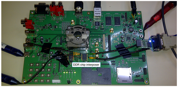
Figure 1: Embedded systems such as IoT devices often require chip interposers to gain access to signal lines on DDR memory
Figure 1 depicts an embedded-system board that encompasses a number of serial-data standards, including DDR3, HDMI, Ethernet, and USB. The DDR3 chip, near the center of the board, has solder-in probes connected to it by means of an interposer (Figure 1).
Figure 2: Interposers reside between the ball-grid array on the bottom of a DDR chip and the PCB's solder pads to make signal lines more easily accessible to probing
Interposers come into play with DDR memory chips on IoT devices because such chips are often made in ball-grid-array (BGA) packages, which renders the signal pins inaccessible. Figure 2 shows DDR chips with and without an interposer as well as an interposer without chip attached. From these images, you get the idea of what the interposer does, which is to bring out formerly inaccessible signals so that they can be probed with relative ease.
Figure 3: A side view of a chip interposer provides a better look at its mechanical function
The rendering of Figure 3 reveals more clearly how the interposer functions mechanically. It's installed by soldering the bottom side to the DDR's BGA footprint on the PC board where the memory chip itself would usually be soldered. The memory chip itself is soldered to the top side of the interposer, either with or without a socket. Interposers can be most useful in applications like IoT devices and other embedded systems, which are typically laid out in dense configurations with other IC packages tightly adjacent to the DDR memory devices.
The JEDEC standard for DRAM testing requires that the device be probed directly at its pins. Alas, at times not even interposers can make this possible. You end up having to probe the signal line somewhere mid-bus rather than at the terminated DRAM chip. Say, for instance, that a read signal emanating from the memory chip is probed mid-bus. The probe picks up some of that signal, but it also continues down the trace to the memory controller, where it reflects back to the probe as a phase-shifted, amplitude-attenuated version of itself and gets mixed in with what the probe is picking up.
Figure 4: Virtual-probing software running on the oscilloscope can remove reflections from mid-bus probing of the bus
The answer to this dilemma is in a technique known as virtual probing. Referring to Figure 4, the bus might be physically probe at mid-bus (as represented by the location of the red probe), but the measurement will be as if the probe was at the DRAM pins, sans reflections (as represented by the grey probe). At top right in Figure 4 is what the signal would look like if probed with the red probe: an eye diagram distorted by reflections, while at top left is the virtual-probed signal, with the eye opened by the virtual-probing software residing on the oscilloscope.
There are two ways in which the virtual-probing software can approach the elimination of mid-bus probing reflections. One is to use S-parameters to model the signal path and remove the reflections through S-parameter modeling. If S-parameters are unavailable, another approach is to use simulation to arrive at RLC models of parameters such as skin effect and delay.
A final post to come will look at some concrete debug steps for IoT DDR memory.
Previous blogs in this series:
IoT Digital Power Management and Power Integrity
Investigating IoT Wireless Signals
Investigating IoT Wireless Signals (Part II)
Acquiring and Characterizing IoT Sensor Signals
Debugging Low-Speed Serial Data on IoT Devices


