


Our last post considered some broad aspects of debugging DDR memory on Internet of Things (IoT) devices, such as how chip interposers can help with probing access and the benefits of virtual probing software. Let's now take a look at some particular examples of problems with these memory chips and their controllers and see how debugging with an oscilloscope might be approached.
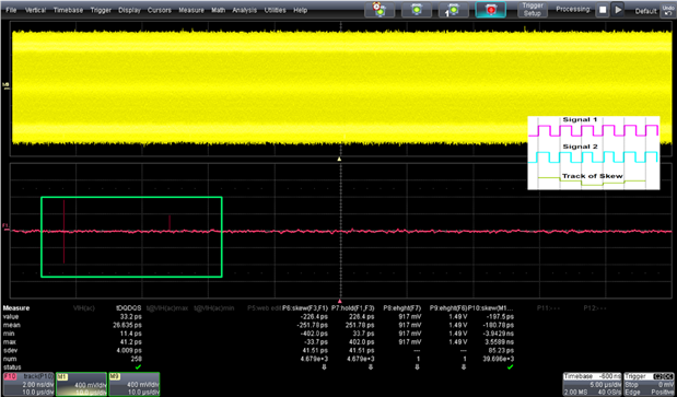
Figure 1: Using the oscilloscope's Track math function can help pin down timing anomalies
Figure 1 is a screen shot from an actual end-user's DUT. The DDR memory was behaving oddly, so measurements were taken of the skew between clock and data and between clock and strobe. They used the oscilloscope's Track math function to plot the measurements in time-coherent fashion against the source trace. Essentially, you end up with a waveform composed of all of the measurement instances of whatever parameter is being measured as a plot vs. time.
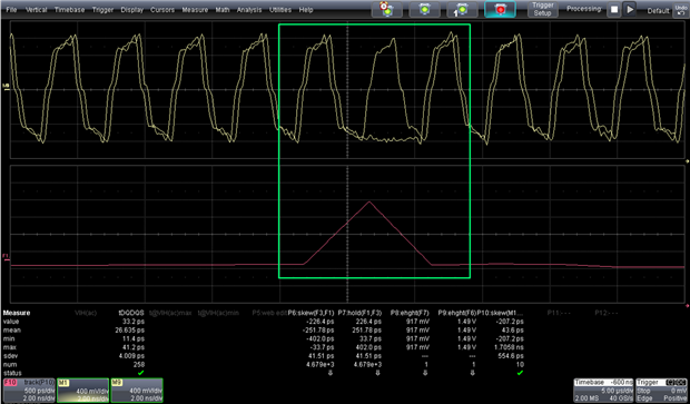
Figure 2: The parameter Track function reveals the cause of the timing problem of Figure 1: a missing clock cycle
In this case, the Track waveform is a plot of the two skews, and you can see some spikes within the green box. Figure 2 reveals the cause of the spikes in the skew-to-skew Track waveform: a missing clock cycle. The end user wasn't aware of this issue, but the Track function is an example of a tool that can help determine why data isn't being transmitted correctly.
An extremely useful tool for DDR debug is the HDA125 high-speed digital analyzer, which can be used with Teledyne LeCroy's DDR Debug Toolkit to perform some highly insightful mixed-signal analysis. The HDA125 can give you a close look at the DDR command bus.
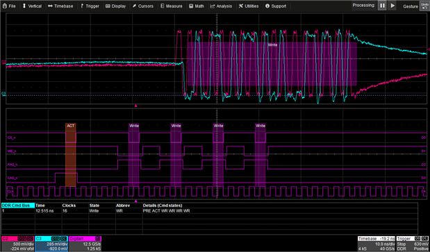
Figure 3: The HDA125 high-speed digital analyzer enables triggering on the state of the DDR command bus
For example, Figure 3 is a screen grab of an instance where there's a command to activate a DDR memory bank followed by four write requests. The HDA125 enables you to trigger on, acquire, and visualize the state of the command bus in this fashion. The top trace in Figure 3 is acquired with analog probes, while digital lines show us what's taking place on the command bus below. This provides the ability, with great certainty, to lock onto reads and writes separately, an important facility when you consider that with DDR memory, reads and writes have separate eye patterns.
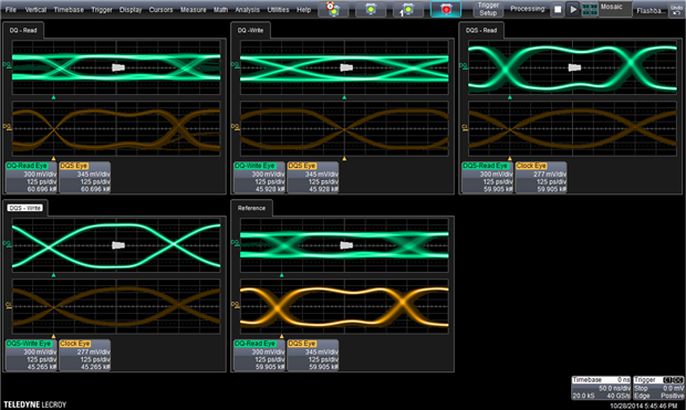
Figure 4: Eye-diagram comparisons are an invaluable DDR debugging tool
For DDR debugging purposes, it is useful to look at reads and writes at the same time. Figure 4 depicts a number of eye-pattern comparisons, such as read vs. clock, read vs. strobe, write vs. clock, and write vs. strobe. There's also an instance of comparing an eye pattern that could be from a device tested the day before with today's results. This is another capability made possible by teaming the HDA125 analyzer with the DDR Debug Toolkit and a suitably capable Teledyne LeCroy oscilloscope.
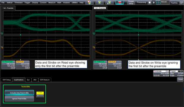
Figure 5: Shown are examples of eye diagrams of isolated portions of the DDR signal burst
Another useful tactic is to perform analysis on the DDR bus by looking at isolated portions of the burst. For example, we might want to see an eye diagram of only the portion of the burst when the DDR signal is coming out of electrical idle. Or, conversely, perhaps we want to ignore that period of the burst and only focus on the DDR signal when it's at either its high or low values. Figure 5 shows examples of both of these scenarios.
Previous blogs in this series:
IoT Digital Power Management and Power Integrity
Investigating IoT Wireless Signals
Investigating IoT Wireless Signals (Part II)
Acquiring and Characterizing IoT Sensor Signals
Debugging Low-Speed Serial Data on IoT Devices
Debugging CANbus for IoT Devices