element14 Community
element14 Community
    Register Log In
  • Site
  • Search
  • Log In Register
  • About Us
  • Community Hub
    Community Hub
    • What's New on element14
    • Feedback and Support
    • Benefits of Membership
    • Personal Blogs
    • Members Area
    • Achievement Levels
  • Learn
    Learn
    • Ask an Expert
    • eBooks
    • element14 presents
    • Learning Center
    • Tech Spotlight
    • STEM Academy
    • Webinars, Training and Events
    • Learning Groups
  • Technologies
    Technologies
    • 3D Printing
    • FPGA
    • Industrial Automation
    • Internet of Things
    • Power & Energy
    • Sensors
    • Technology Groups
  • Challenges & Projects
    Challenges & Projects
    • Design Challenges
    • element14 presents Projects
    • Project14
    • Arduino Projects
    • Raspberry Pi Projects
    • Project Groups
  • Products
    Products
    • Arduino
    • Avnet Boards Community
    • Dev Tools
    • Manufacturers
    • Multicomp Pro
    • Product Groups
    • Raspberry Pi
    • RoadTests & Reviews
  • Store
    Store
    • Visit Your Store
    • Choose another store...
      • Europe
      •  Austria (German)
      •  Belgium (Dutch, French)
      •  Bulgaria (Bulgarian)
      •  Czech Republic (Czech)
      •  Denmark (Danish)
      •  Estonia (Estonian)
      •  Finland (Finnish)
      •  France (French)
      •  Germany (German)
      •  Hungary (Hungarian)
      •  Ireland
      •  Israel
      •  Italy (Italian)
      •  Latvia (Latvian)
      •  
      •  Lithuania (Lithuanian)
      •  Netherlands (Dutch)
      •  Norway (Norwegian)
      •  Poland (Polish)
      •  Portugal (Portuguese)
      •  Romania (Romanian)
      •  Russia (Russian)
      •  Slovakia (Slovak)
      •  Slovenia (Slovenian)
      •  Spain (Spanish)
      •  Sweden (Swedish)
      •  Switzerland(German, French)
      •  Turkey (Turkish)
      •  United Kingdom
      • Asia Pacific
      •  Australia
      •  China
      •  Hong Kong
      •  India
      •  Korea (Korean)
      •  Malaysia
      •  New Zealand
      •  Philippines
      •  Singapore
      •  Taiwan
      •  Thailand (Thai)
      • Americas
      •  Brazil (Portuguese)
      •  Canada
      •  Mexico (Spanish)
      •  United States
      Can't find the country/region you're looking for? Visit our export site or find a local distributor.
  • Translate
  • Profile
  • Settings
Personal Blogs
  • Community Hub
  • More
Personal Blogs
Legacy Personal Blogs Instrument Control Board - Prototyping the Power section
  • Blog
  • Documents
  • Mentions
  • Sub-Groups
  • Tags
  • More
  • Cancel
  • New
  • Share
  • More
  • Cancel
Group Actions
  • Group RSS
  • More
  • Cancel
Engagement
  • Author Author: Andrew J
  • Date Created: 8 Nov 2020 6:56 PM Date Created
  • Views 4089 views
  • Likes 9 likes
  • Comments 24 comments
Related
Recommended

Instrument Control Board - Prototyping the Power section

Andrew J
Andrew J
8 Nov 2020

Introduction

This post is continuing the series on creating a control board for an electronic load.  Having created a prototype board to test various configurations of features, described in this post, I have spent some time evaluating the Power section with the aim of minimising output ripple and noise on the power lines.  One aspect of this is to try and understand more about ripple and noise as I find it a bit of a head-scratcher - a lot of information on this topic is maths and concept heavy which I struggle with so I'm hoping that experimenting will help.


TL;DR;

I have taken a number of pre- and post-change measurements to see the impact of those changes and see how much I can attenuate ripple and noise.  Within the scope of my knowledge, I've been reasonably successful.  The 12Vout power still has a sizeable amount of ripple and noise but this line is only to drive a fan so I'm not too concerned about it.  The post is mostly images.


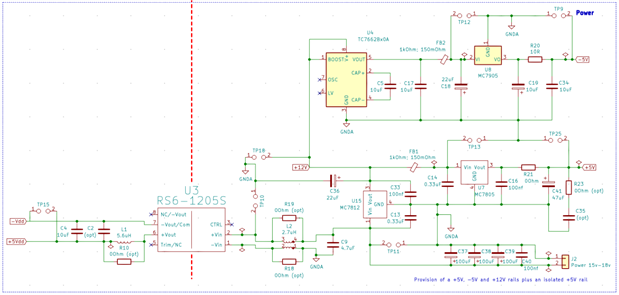
Power Section Circuit

(See this post for the full circuit.)

image

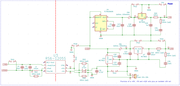
This is intended to provide the following power rails:

  • +15Vin: to drive the power section.
  • +5V: to power DACs, ADCs and other ICs
  • -5V: to provide a -ve source for Op Amps to enable rail-to-rail operation down to 0V
  • +12V: to provide a source to drive a fan.  It also provides a source for the +5V regulator and the DC-DC charge pump which inverts it for driving the -5V regulator
  • +5Vdd: to provide an isolated +5V source to drive a microcontroller and signal isolation ICs.  This is generated from a DC-DC isolating convertor.

The critical power rails are the +5V and -5V which drive the sensitive ICs.


Measurements

I'm taking 'before' and 'after' measurements to compare against changes I make.  As I haven't populated the downstream components, I have provided a load as follows:

  • A measured 285Ohm resistor soldered across TP9 for the -5Vout
  • A measured 317Ohm resistor soldered across TP25 for the +5Vout
  • A 4Duino attached to the board driven by the +5Vdd output.

In the notes below, I don't comment on everything I tried, just what I ended up with.


Ripple and noise are load-dependent.  That means that what I measure and change in this testing will have to be revisited once I fully populate the other sections of the prototype board.
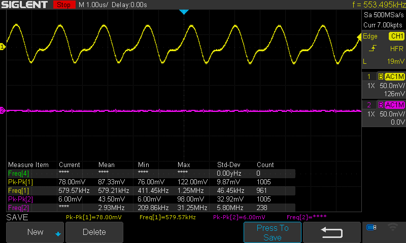
 

Before

I wanted to see the impact of adding in the inductor, choke and ferrite beads so the board is populated as follows.  All components in place except for:

  • L1: NOT populated
  • R10: Populated with 0Ohm jumper
  • L2: NOT populated
  • R18 and R19: Populated with 0Ohm jumper
  • FB1 and FB2: Populated with 0Ohm jumper and NOT a ferrite bead
  • R22, R23, C34 and C35: Not populated
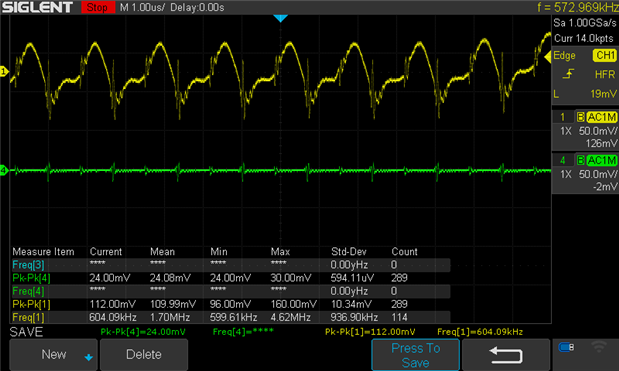
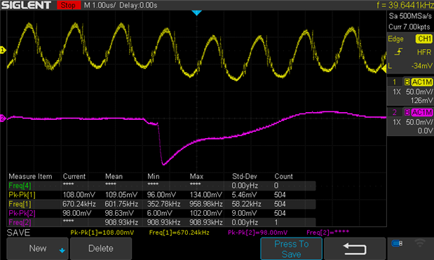
 

Image 1:

Ch1: +15Vin

Ch2: +12Vout

image

I'm driving the board with a relatively cheap 15V 1.2A switching supply.  Nominally, it has a 150mVpp specification but that's under a very specific condition.  Here, it's not too bad at 87mV.  I should have expanded the 12V signal to better see it but the measurement is showing quite a range on the ripple.
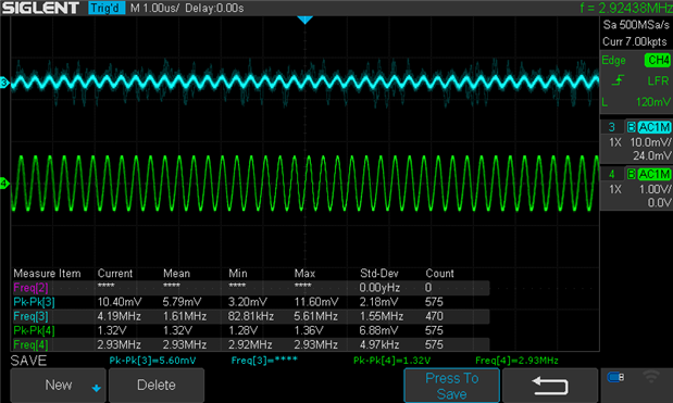
 

Image 2:

Ch3: +5Vout

Ch4: -5Vout

image

The +5Vout is picking up what I assume is switching noise propagated through the 12V regulator but has attenuated the ripple considerably.  The -5Vout is a disaster and, in actual fact, is worse than shown as I mistakenly measured at x1 but left the probe switched at x10 - peak to peak ripple is actually 1.32V.  Clearly, something is wrong.


Image 3:

Ch1: +15Vin

Ch4: +5Vdd DC-DC isolator output

image

Interestingly, the 15Vin measurement is showing noise here which isn't apparent in Image 1.  The measurement in this image is taken at TP10, rather than TP11 in image 1 - I wouldn't have thought it made a difference but I suspect here, it's picking up noise from the RS6 DC-DC isolator.  As above, I should have expanded the +5Vdd signal but the measurement is showing a consistent 24mV noise range with ringing from the isolator and is in-step with the +15Vin signal.
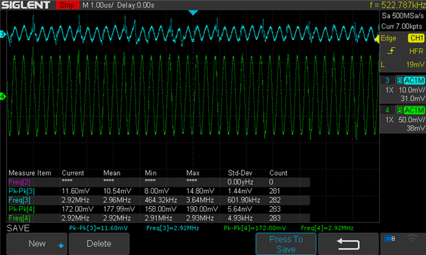
 

After

The following measurements are taken once I've made the following changes:

  • L1: Populated
  • R10: NOT populated
  • L2: Populated
  • R18 and R19: NOT populated
  • FB1 and FB2: Populated with ferrite beads

I also added, off-board, 3x100uF electrolytic capacitors plus a 0.1uF mlcc to the +15Vin line.


Image 4

Ch1: +15Vin

Ch2: Ignore

image

The additional capacitance doesn't seem to make much of a difference - it's smoothed out the signal rise but the overall peak-peak measurement is worse.  Still showing noise.


Image 5

Ch3: +5Vout

Ch4: -5Vout

image

The board population has had a positive impact on the +5Vout signal although there is still ripple and noise.  -5Vout is being measured properly here and shows how bad it actually is compared to image 2.  The regulator is oscillating and not at all stable - as discussed in this post.


Image 6

Ch3: Output of the DC-DC inverter

Ch4: -5Vout

image

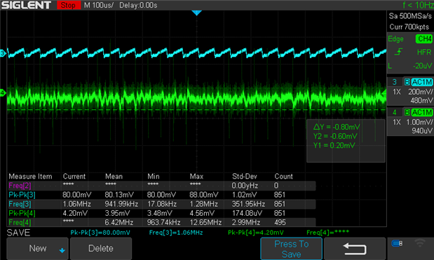
The -5Vout signal was oscillating because of an assumption I made regarding the ESR of the output capacitor so I replaced the C19 1uF output mlcc for a 10uF electrolytic capacitor and placed a 22uF electrolytic capacitor in parallel to C18.  That has stabilised the output and reduced the ripple down to 800uV with noise peak to peak of 3.95mV (mean.)  The 22uF capacitor also had a significant impact on the ripple output from the DC-DC investor which was 320mV peak to peak beforehand (no image in this post.)
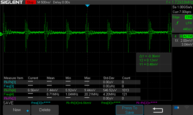
 

Image 7

Ch3: Output of the DC-DC inverter

Ch4: -5Vout

image

To try and improve this further, I added a 10Ohm/10uF mlcc low pass filter after the -5V regulator (R20 populated with 10Ohm, R22 populated with 10uF and C34 populated with 0Ohm jumper.)  I also removed C18 0.33uF capacitor leaving just the 22uF capacitor for input.  This has reduced ripple to 680uV and noise peak to peak to 2.83mV (mean).  The LPF has reduced the output voltage from -5.011V to -4.85V but given its purpose - the negative input to OpAmps - this is not an issue.


Image 8

Ch3: 12Vout (+5V regulator in)

Ch4: +5Vout

image

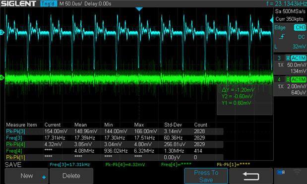
This is a better view of the 12Vout signal which is very noise.  The 5V regulator deals with it pretty well giving a ripple of 1.2mV with noise peak to peak of 3.85mV (mean.)


Image 9

Ch3: 12Vout (+5V regulator in)

Ch4: +5Vout

image

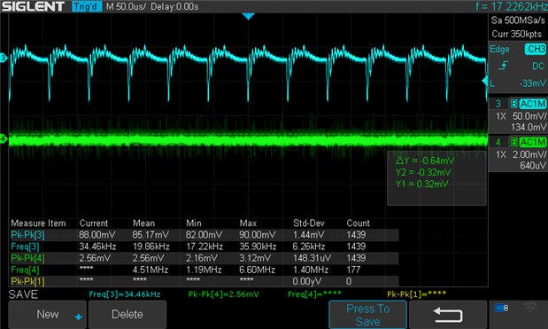
To try and address the 12V regulator output ripple, I added a 22uF electrolytic capacitor in parallel to C33, it's output capacitor.  Additionally, I added a 47uF electrolytic capacitor to +5Vout in parallel to C16 (a smaller capacitor made no difference and a larger one made it worse.)  This seems to have reduced the ripple to 640uV and noise peak to peak to 2.56mV (mean.)


Image 10

Ch4: +5Vdd DC-DC Isolator output

image

This is a better view of the output from the RS6 isolator.  The overall changes made across the board does seem to have had a positive impact on this signal, presumably because the input signal is cleaner (??)  Still noisy though, although the 4Duino doesn't seem to mind.  It may be an issue for the I2C and Digital isolators though which I'll discover as I move the prototype forward - initial breadboarding with these components hasn't shown a problem though.


Final Changes

The circuit now looks like this, with the changes highlighted.

image

Summary

It does feel that I've made a reasonable stab at attenuating ripple and noise on the +5Vout and -5Vout lines, and +5Vdd isn't too bad (certainly, the 4Duino works without issue.)  The 7805 and 7905 regulators are not the best (but what I'm used to) and I'm contemplating looking at other regulators such as AD LT1964 and AD ADP3338.  I'd need to create another PCB but it may make an interesting comparison!


I've reached the limit of my knowledge but I also wonder if there's more to be gained for the purposes the power lines will be used for - I'm open to opinions and ideas, please comment below!


Further Posts

Creating an Instrument Control Board

Instrument Control Board - Component Selection

Instrument Control Board - Prototyping the Power section (this post)

  • Sign in to reply

Top Comments

  • michaelkellett
    michaelkellett over 4 years ago +5
    If you add LC filters with large inductors you can very easily get issues with large voltage overshoots at switch on. You can mitigate this by carefully placed additional resistance to reduce the Q of…
  • michaelkellett
    michaelkellett over 4 years ago in reply to Andrew J +5
    The design with the 470uF is for a power amplifier which draws a good bit more current. The values of 680uH and 100uF are chosen for maximum inductance in a reasonable (quite small) size. The current drawn…
  • fmilburn
    fmilburn over 4 years ago +3
    Hi Andrew, Nicely done. I am always impressed with the thought you put into your designs and the documentation. Frank
Parents
  • michaelkellett
    michaelkellett over 4 years ago

    If you add LC filters with large inductors you can very easily get issues with large voltage overshoots at switch on. You can mitigate this by carefully placed additional resistance to reduce the Q of the LC filter but this will often reduce its filtering effect as well. An alternative is to use zener diodes to clamp the rail but beware that there will be a large difference between the zener clamping voltage and its "zero" current voltage.

    image


    This is the power supply from one of my designs - L2 and L3 are Bourns SRR0735A-681M and C90 and C91 are 100uF 10V polymer electrolytics with ESR about 0.016 ohms. (Kemet A758EK107M1AAAE016).

    The zeners are 5.1V BZX84.


    MK

    • Cancel
    • Vote Up +5 Vote Down
    • Sign in to reply
    • More
    • Cancel
  • Andrew J
    Andrew J over 4 years ago in reply to michaelkellett

    Hi Michael,


    Despite what I said in my last comment about leaving the -5V rail with a RC filter, and as I'm going to re-do the PCB, I'm feeling inclined to build up two versions of the +5V and -5V rails.  I've been looking at your circuit and I think it would be interesting to compare the two.  I did have some questions though to help my understanding.


    You did say you liked "real filters with big inductors and caps"!  Do such large sizes have any other implications besides the overshoots (and ignoring cost/board space implications)?  The cut-off frequency of the filter is 610Hz and the resonant frequency is also 610Hz - was the values selected to do that?  I assume that any noise at that frequency will be magnified but higher frequency noise is going to be attenuated so where the noise is high-frequency, the low resonance frequency isn't much of an issue?


    The 3.3V regulator is fed from the filtered +5V output so I assume its output has the same low ripple/noise as the +5V output?


    You mentioned "...but beware that there will be a large difference between the zener clamping voltage and its "zero" current voltage".  I don't really understand what you mean and I haven't been able to figure it out by reading about zeners in more detail.  Could you explain a bit more please.


    You'd shown this on an earlier post and gave the values of the output caps on the regulators as 470uF.  I'd not even considered such high capacitance values on the output of the regulators - were these chosen for the requirements of your supply or something you again "like to have"? 


    The TPS60403 is an unregulated charge pump inverter and you are feeding it from your 5V regulator (pre filter.)  In my circuit I actual run the +12V through a charge pump inverter and then a -5V regulator.  This is to generate a -5V rail for opamps - a 'typical load' in the TPS datasheet.  Although the output is unregulated, given its purpose I don't see a problem with doing the same with my circuit and saving a number of components (the -5V regulator and its supporting capacitors) - I presume the output LC filter handles the noise and ripple well?

    • Cancel
    • Vote Up +3 Vote Down
    • Sign in to reply
    • More
    • Cancel
  • Andrew J
    Andrew J over 4 years ago in reply to michaelkellett

    Not to worry image 


    I'd still like to understand about the zener zero current.


    I also asked about the +3.3V being fed from the filtered output of the +5V but realise I'd misread the schematic!  I assume the quality of the 3.3V output was sufficient for your need here, but would there have been an issue with feeding that from the +5V filter?  I would have thought doing that would provide a quality output on V3.3.  This is what I was thinking as equivalent for my need:


    12Vout --|-> LC Filter |-> LM7805 -------------------> +5V output

                   |                   |--------------------------------> +12V output

                   |-> Chg Amp Inv -> LM7905 -> LC Filter -> -5V output

    • Cancel
    • Vote Up 0 Vote Down
    • Sign in to reply
    • More
    • Cancel
  • michaelkellett
    michaelkellett over 4 years ago in reply to Andrew J

    It depends on the application - in mine the 3.3V is for logic (mainly processor) which is not fussy re. noise but will use lots of current, the +/- 5V supplies are for analogue and are susceptible to noise.

    Sharing the filter is OK but only if the total current is not too high, on my design the 3.3V current was way higher the the 5V current so the 200mA rated inductor would have struggled.


    MK

    • Cancel
    • Vote Up +1 Vote Down
    • Sign in to reply
    • More
    • Cancel
  • Andrew J
    Andrew J over 4 years ago in reply to michaelkellett

    Ok, makes sense - I can work that through my design.

    • Cancel
    • Vote Up 0 Vote Down
    • Sign in to reply
    • More
    • Cancel
  • jc2048
    jc2048 over 4 years ago in reply to Andrew J

    I'd still like to understand about the zener zero current.

    This is from a Vishay datasheet for the BZX84 series of Zener diodes.


    image


    You can see that, for the true zeners, the clamping is quite soft. It gets better above 5V, where the avalanche-breakdown effect dominates.


    So, the 3.3V zener might clamp to 3.3V at the test current of 5mA, but it's over 4V with even just 50mA flowing through it.

    • Cancel
    • Vote Up +2 Vote Down
    • Sign in to reply
    • More
    • Cancel
  • Andrew J
    Andrew J over 4 years ago in reply to jc2048

    Thanks Jon, that's useful.  So a rail with 40mA on it would be clamped to 4V by a 3.3V Zener; with a very small amount of current it would clamp it to 2V.  For a 5.6V zener, at close to zero current it would be clamping the rail to 5V.


    "An alternative is to use zener diodes to clamp the rail but beware that there will be a large difference between the zener clamping voltage and its "zero" current voltage."

    This is the sentence I am/was struggling to get my head around in relation to using a zener to clamp a rail against a high inrush voltage.  Let's say I have a 3.3V rail with an inductor.  At turn on, inrush voltage briefly rises to 6V so I use a 3.3V zener after the inductor to (in theory) clamp the rail to 3.3V.  The chart shows that actually a 3.3V BZX84 zener would clamp from 2V @ 'zero' mA to 4.2V @ 50mA and above, give or take. 


    From that chart and your explanation, I think the implication is that if I have a load that draws say, 700uA at 3.3V then the zener will clamp the rail to 2V and thus my load isn't going to work. I'd need to, say, add a resistance in parallel to the load to ensure that 5mA, preferably, was being drawn in order to ensure operation of my actual load?  In other words, before putting a zener into the circuit, ensure I understand its breakdown characteristics vs the load and design accordingly?

    • Cancel
    • Vote Up 0 Vote Down
    • Sign in to reply
    • More
    • Cancel
Comment
  • Andrew J
    Andrew J over 4 years ago in reply to jc2048

    Thanks Jon, that's useful.  So a rail with 40mA on it would be clamped to 4V by a 3.3V Zener; with a very small amount of current it would clamp it to 2V.  For a 5.6V zener, at close to zero current it would be clamping the rail to 5V.


    "An alternative is to use zener diodes to clamp the rail but beware that there will be a large difference between the zener clamping voltage and its "zero" current voltage."

    This is the sentence I am/was struggling to get my head around in relation to using a zener to clamp a rail against a high inrush voltage.  Let's say I have a 3.3V rail with an inductor.  At turn on, inrush voltage briefly rises to 6V so I use a 3.3V zener after the inductor to (in theory) clamp the rail to 3.3V.  The chart shows that actually a 3.3V BZX84 zener would clamp from 2V @ 'zero' mA to 4.2V @ 50mA and above, give or take. 


    From that chart and your explanation, I think the implication is that if I have a load that draws say, 700uA at 3.3V then the zener will clamp the rail to 2V and thus my load isn't going to work. I'd need to, say, add a resistance in parallel to the load to ensure that 5mA, preferably, was being drawn in order to ensure operation of my actual load?  In other words, before putting a zener into the circuit, ensure I understand its breakdown characteristics vs the load and design accordingly?

    • Cancel
    • Vote Up 0 Vote Down
    • Sign in to reply
    • More
    • Cancel
Children
  • jc2048
    jc2048 over 4 years ago in reply to Andrew J

    I think you're taking Michael too literally. I presume he meant the low current that the voltage is characterised at, in this case 5mA, rather than actually zero. If you were using the diode as a voltage reference, that's the current you'd run through the part to give a reasonably accurate voltage. But if you're trying to use the device to clamp a transient, where the instantaneous current that might pass through the device is potentially quite high, then the voltage that it limits to is going to be a good bit higher.


    He was just warning you to not expect it to be a rock-hard clamp at the voltage written on the device.


    As you've understood, the zener voltage is going to have to be higher than the rail voltage or the diode will be conducting significantly all the time and, with a small zener like the BZX84, that would then lead you to problems with the device dissipation, even if it didn't drag the rail down.


    In a situation like this [transient suppression on a power rail], you might also want to look at TVS devices. They are zeners too, but they're engineered to be more robust.

    • Cancel
    • Vote Up +2 Vote Down
    • Sign in to reply
    • More
    • Cancel
  • Andrew J
    Andrew J over 4 years ago in reply to jc2048

    Thanks Jon, got it now.

    • Cancel
    • Vote Up +1 Vote Down
    • Sign in to reply
    • More
    • Cancel
element14 Community

element14 is the first online community specifically for engineers. Connect with your peers and get expert answers to your questions.

  • Members
  • Learn
  • Technologies
  • Challenges & Projects
  • Products
  • Store
  • About Us
  • Feedback & Support
  • FAQs
  • Terms of Use
  • Privacy Policy
  • Legal and Copyright Notices
  • Sitemap
  • Cookies

An Avnet Company © 2025 Premier Farnell Limited. All Rights Reserved.

Premier Farnell Ltd, registered in England and Wales (no 00876412), registered office: Farnell House, Forge Lane, Leeds LS12 2NE.

ICP 备案号 10220084.

Follow element14

  • X
  • Facebook
  • linkedin
  • YouTube