element14 Community
element14 Community
    Register Log In
  • Site
  • Search
  • Log In Register
  • Community Hub
    Community Hub
    • What's New on element14
    • Feedback and Support
    • Benefits of Membership
    • Personal Blogs
    • Members Area
    • Achievement Levels
  • Learn
    Learn
    • Ask an Expert
    • eBooks
    • element14 presents
    • Learning Center
    • Tech Spotlight
    • STEM Academy
    • Webinars, Training and Events
    • Learning Groups
  • Technologies
    Technologies
    • 3D Printing
    • FPGA
    • Industrial Automation
    • Internet of Things
    • Power & Energy
    • Sensors
    • Technology Groups
  • Challenges & Projects
    Challenges & Projects
    • Design Challenges
    • element14 presents Projects
    • Project14
    • Arduino Projects
    • Raspberry Pi Projects
    • Project Groups
  • Products
    Products
    • Arduino
    • Avnet & Tria Boards Community
    • Dev Tools
    • Manufacturers
    • Multicomp Pro
    • Product Groups
    • Raspberry Pi
    • RoadTests & Reviews
  • About Us
  • Store
    Store
    • Visit Your Store
    • Choose another store...
      • Europe
      •  Austria (German)
      •  Belgium (Dutch, French)
      •  Bulgaria (Bulgarian)
      •  Czech Republic (Czech)
      •  Denmark (Danish)
      •  Estonia (Estonian)
      •  Finland (Finnish)
      •  France (French)
      •  Germany (German)
      •  Hungary (Hungarian)
      •  Ireland
      •  Israel
      •  Italy (Italian)
      •  Latvia (Latvian)
      •  
      •  Lithuania (Lithuanian)
      •  Netherlands (Dutch)
      •  Norway (Norwegian)
      •  Poland (Polish)
      •  Portugal (Portuguese)
      •  Romania (Romanian)
      •  Russia (Russian)
      •  Slovakia (Slovak)
      •  Slovenia (Slovenian)
      •  Spain (Spanish)
      •  Sweden (Swedish)
      •  Switzerland(German, French)
      •  Turkey (Turkish)
      •  United Kingdom
      • Asia Pacific
      •  Australia
      •  China
      •  Hong Kong
      •  India
      • Japan
      •  Korea (Korean)
      •  Malaysia
      •  New Zealand
      •  Philippines
      •  Singapore
      •  Taiwan
      •  Thailand (Thai)
      • Vietnam
      • Americas
      •  Brazil (Portuguese)
      •  Canada
      •  Mexico (Spanish)
      •  United States
      Can't find the country/region you're looking for? Visit our export site or find a local distributor.
  • Translate
  • Profile
  • Settings
Personal Blogs
  • Community Hub
  • More
Personal Blogs
John Wiltrout's Blog Reverse Engineering integral DC Converters
  • Blog
  • Documents
  • Mentions
  • Sub-Groups
  • Tags
  • More
  • Cancel
  • New
  • Share
  • More
  • Cancel
Group Actions
  • Group RSS
  • More
  • Cancel
Engagement
  • Author Author: jw0752
  • Date Created: 6 Mar 2016 11:46 PM Date Created
  • Views 2412 views
  • Likes 6 likes
  • Comments 24 comments
  • dc-dc converter
  • reverse_engineering
Related
Recommended

Reverse Engineering integral DC Converters

jw0752
jw0752
6 Mar 2016

The other day while trouble shooting a control panel from a Pelton Crane Delta Q Dental Sterilizer I noticed that two of the required voltages were not being supplied by the main power supply but were instead being synthesized by a small group of components on one end of the circuit board. The display on the sterilizer was totally dark and the problem was going to be in one of 2 boards. The ultimate decision we faced was which of the two boards costing $1000. and $600 respectively was bad. Unfortunately they would not be returnable if we guessed wrong and ordered the wrong board. Through a process of elimination I was able to determine that the problem was in some of the OEM components on the more expensive board. When I had gone as far as I could towards fixing the problem we broke down and ordered a new board.


My interest had however been captivated by the small group of components on one end of the board that was responsible for taking  +12 and  + 5 volt input supplies and outputting 24 volts and 40 volts to be used in the OLED display circuitry. Here is a picture of the board of interest and a closeup of the section responsible for the voltage conversion. At this time I had not yet realized that I was dealing with two distinct converters.


image

Over View of Display driver board


image

Closeup of 24V and 40V synthesis section


image

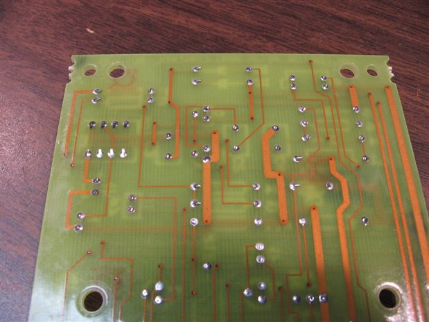
Back side of the board. This is a two layer board fortunately.


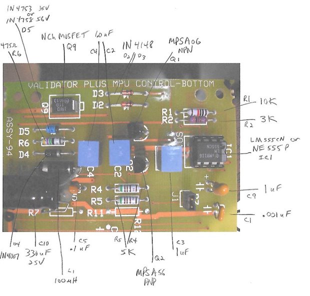
My first step to reverse engineering the circuit was to identify each of the components and to label a layout of the board. Fortunately I found that none of the components were OEM and that all were common and available in the shop parts supply. Where appropriate to understanding the circuit, Data Sheets were accessed. Here is the parts layout with labels.


image


The next step in the reverse engineering process is to create a schematic. This involves getting the component symbols on paper and determining their interconnections. For me this means a lot of time flipping the circuit board back and forth from front to back, visually tracing the the traces and vias, and using the ohm meter to verify connections. After a while, a rough draft of the schematic is produced by hand. A close inspection of the schematic and application of circuit logic often forces me back to the board to make sense of the circuit and to correct obvious gaps.


image


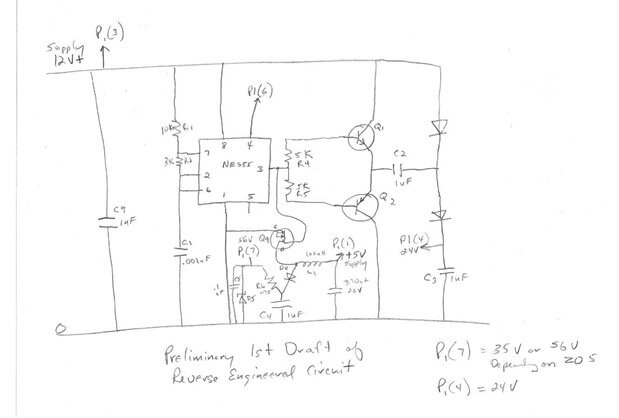
While it is possible to work off a crude schematic like this I always like to clean up the work and make a CAD schematic. Obviously, I got into a little trouble in the lower center of the hand produced schematic and we will clean up this section in the CAD production. Drawing freehand while reverse engineering a board usually leads to a messy first draft. Here is a CAD rendition.


image

With the schematic in hand it became clear that we actually had two converters on this board working off a single astable multivibrator. The 555 timer in this case is providing a 67 kHz 12 volt square wave. The section of the circuit that produces the 24 volt output uses this signal to drive a push pull set of NPN PNP general purpose transistors. The transistors in turn drive a voltage doubler with a 24 volt output. The 40 volt output is produce by driving an N Ch MOSFET with the 555 signal. The input voltage for this section is only 5 volts. When the MOSFET is in saturation energy is stored in the 100 uH inductor L1. When the MOSFET turns off this energy is released through diode D4 and stored in capacitor C4. Since the impedance is quite high the voltage is also quite high. Resistor R6 limits the current to Zener diode D5 which serves as a voltage regulator. Output in this case 40 volts is taken from the point in the circuit marked P1(7). C5 helps to decouple transients and noise from the output. C10 provides a reserve of current to L1 when the MOSFET turns on.


It is interesting to note that this design has been used by the sterilizer company for over a decade. When the board was first designed a 56 volt supply was needed and the requisite Zener diode was used to produce this voltage. As the technology of the OLEDs has improved the current required voltage became 35 volts and the only change to the circuit was the use of a 35 volt Zener. My rendition of the circuit creates 40 volts but this is only because my parts bins only had (2) 20 volt Zeners in this higher voltage range so I put them in series to approximate the actual circuit.


Now that we have the schematic the fun begins as we will bread board the circuit from the schematic to see if it will work as hoped. Here is a picture of the circuit bread boarded. Fortunately, except for the Zener, I had all the correct value components in the bins so I did not have to place an order.


image


image


For my initial test I have supplied +12 volts to the main rail and +5 volts to the MOSFET section of the circuit. I have an oscilloscope monitoring the output of the 555 astable multivibrator and I have DVMs on the 24 volt and 40 volt outputs. This is very unusual for me but it actually worked the first time. No Smoke, No Fire!  Here are the outputs as displayed by the test instruments.


image

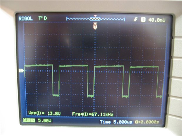
Sorry for the poor image. I was too lazy to export the image and just took a picture of it.


image

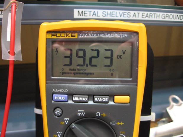
This is my 40 volt output point. Since I am using 2 Zeners in series and probably do not have them in their optimal operation mA range I feel the 39.23 V is acceptable.


image

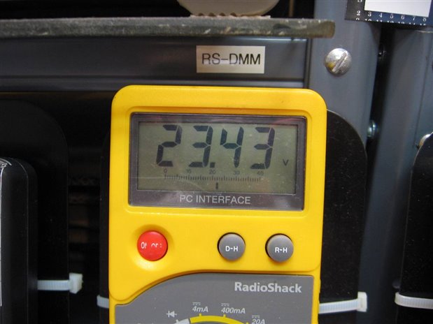
The regulation of this output is tied to the regulation of the 12 volt input of the circuit and I am very pleased with how close it came to 24 volts. The circuits that are using these voltage supplies are not precision and can tolerate a range of voltage.


The last thing that I did was to load the 40 volt circuit with a 10 K resistor and measured the voltage drop. The 10 K load produced a 2.39 Volt drop. Calculations indicated that the supply has an approximate 650 ohm ESR. At least 475 ohms of this ESR is the series current limiting resistor. I have left the test jig set up on the bench and will play with it for a couple days before tear down. I found this exercise helpful as I can see application of the concepts used in these 2 voltage converters will be useful in future designs.


John


  • Sign in to reply

Top Comments

  • mcb1
    mcb1 over 9 years ago in reply to jc2048 +3
    I hope we're not encouraginging anyone to design outside the datasheet - a cardinal rule of professional design is that you always work within the parameters set by the manufacturer. Haha .... unless you…
  • shabaz
    shabaz over 9 years ago +2
    Hi John, Excellent work as usual, and very relevant to using modern displays such as OLEDs. All the ones I've encountered need some particular high voltage, so it is good to see the various boost converter…
  • jw0752
    jw0752 over 9 years ago in reply to Jan Cumps +2
    Hi Jan, I have run some experiments with "interesting" results. I modified the circuit so that it was more like your ideal by removing the 40 volt zener diode. The Vg = 5.1 volts, According to the Scope…
Parents
  • Jan Cumps
    Jan Cumps over 9 years ago

    Great great work, jw0752 !!

    The 40 volt part has a classic boost converter in it.

    I've redrawn your schema a little bit to make that more apparent.


    image


    Here's the classic drawing (taken from Analysis of Four DC-DC Converters in Equilibrium )


    classic boost converter

    • Cancel
    • Vote Up +1 Vote Down
    • Sign in to reply
    • More
    • Cancel
  • Jan Cumps
    Jan Cumps over 9 years ago in reply to Jan Cumps

    In theory, the output voltage (before R6) should be:

    V = Vg / (1-D)

    Where V = the output voltage

    Vg the supply voltage (5V)

    D the duty cycle (you could check the duty cycle of the NE555 output with your Rigol's Measure functions, let's say it's 90% here)


    -> V =5V / (1 - 0.9) = 50V


    It would be cool if you could check that duty cycle going into Q9's gate, and the voltage before R6 to see if the equation holds.

    • Cancel
    • Vote Up +1 Vote Down
    • Sign in to reply
    • More
    • Cancel
  • mcb1
    mcb1 over 9 years ago in reply to jw0752

    I have been known to make my share of smoke and fire

    Oven gloves as Personal Protection Equipment ... nice

    • Cancel
    • Vote Up +1 Vote Down
    • Sign in to reply
    • More
    • Cancel
  • jc2048
    jc2048 over 9 years ago in reply to jw0752

    I'll throw in a warning here that you are going to end up with a large capacitor charged to 130V with no real load to discharge it quickly afterwards. I know that you don't need the warning because you used to work with vacuum tubes, but others might not be so aware.


    An alternative to doing the experiment slowly, would be to do it quickly using your scope. If you put a low value resistor (less than an ohm - perhaps start with 0.1) between the source of the FET and ground, the voltage across the resistor would be proportional to the current (and one end is ground so it makes for an easy measurement with the scope). During the time that the FET was on you'd see the current ramp up as the coil established its magnetic field and poured energy into it. Normally, when the FET turned off the current would fall to zero because the coil's energy passes to the output capacitor through the diode, but if the FET diode breaks down you'd see the current ramp down again because the path would now be through the FET.

    • Cancel
    • Vote Up 0 Vote Down
    • Sign in to reply
    • More
    • Cancel
  • jw0752
    jw0752 over 9 years ago in reply to jc2048

    Hi Jon,

    Excellent warning about high voltage on capacitor to everyone including old guys like me. I also like your idea to monitor the current in a source resistor using the scope. I am getting more interesting tests out of this circuit than I originally thought I would.

    John

    • Cancel
    • Vote Up +1 Vote Down
    • Sign in to reply
    • More
    • Cancel
  • jw0752
    jw0752 over 9 years ago in reply to jw0752

    Hi Jon,

    I ran the experiment and found that the current draw on the 5 volt supply was very constant at 110 mA up until the voltage reached 118 Volts. At this point the current draw increased fairly linearly at 10 mA per volt. I also noted that cooling the MOSFET caused a rapid increase to the 250 mA level. Allowing the MOSFET to heat up again would cause the mA draw to once again drop back from the 250 mA level unless the voltage was above 129 Volts. Since we are operating outside the design parameters of the IRF511 I guess I can be pleased that it is working as well and consistently as it is.

    John

    • Cancel
    • Vote Up 0 Vote Down
    • Sign in to reply
    • More
    • Cancel
  • jc2048
    jc2048 over 9 years ago in reply to jw0752

    For a Zener, the temperature coefficient is something like 0.1% per degree, so if this behaves the same and you cool the part with a freezer spray (which I assume is what you mean you did), the change would be several volts downwards in the Zener voltage which would tie in with the current increasing. But it's not quite proof that my guess is right - just suggestive that it might be. What happens above 129V? Does the voltage keep rising?


    So far it's not too stressful for the FET. The power is involved is 1.25W, which the package can manage to deal with without a heatsink, and the current at 129V is less than 10mA average so we aren't into the realms where bond wires are going to melt or anything like that. The energy is limited to what goes into the coil's magnetic field each cycle, so it's not like connecting the device to a PSU that will just blast it to pieces. If you're worried, you could reduce the size of the inductor to reduce the energy further.


    As you say, we're certainly way beyond the design parameters. I hope we're not encouraginging anyone to design outside the datasheet - a cardinal rule of professional design is that you always work within the parameters set by the manufacturer.

    • Cancel
    • Vote Up +2 Vote Down
    • Sign in to reply
    • More
    • Cancel
Comment
  • jc2048
    jc2048 over 9 years ago in reply to jw0752

    For a Zener, the temperature coefficient is something like 0.1% per degree, so if this behaves the same and you cool the part with a freezer spray (which I assume is what you mean you did), the change would be several volts downwards in the Zener voltage which would tie in with the current increasing. But it's not quite proof that my guess is right - just suggestive that it might be. What happens above 129V? Does the voltage keep rising?


    So far it's not too stressful for the FET. The power is involved is 1.25W, which the package can manage to deal with without a heatsink, and the current at 129V is less than 10mA average so we aren't into the realms where bond wires are going to melt or anything like that. The energy is limited to what goes into the coil's magnetic field each cycle, so it's not like connecting the device to a PSU that will just blast it to pieces. If you're worried, you could reduce the size of the inductor to reduce the energy further.


    As you say, we're certainly way beyond the design parameters. I hope we're not encouraginging anyone to design outside the datasheet - a cardinal rule of professional design is that you always work within the parameters set by the manufacturer.

    • Cancel
    • Vote Up +2 Vote Down
    • Sign in to reply
    • More
    • Cancel
Children
  • mcb1
    mcb1 over 9 years ago in reply to jc2048

    I hope we're not encouraginging anyone to design outside the datasheet - a cardinal rule of professional design is that you always work within the parameters set by the manufacturer.

    Haha .... unless you're dealing with Raspberry Pi.

    They seem to have difficulty releasing the GPIO specs.

    https://www.raspberrypi.org/forums/viewtopic.php?f=29&t=138215&hilit=gpio+spec


    Mark

    • Cancel
    • Vote Up +3 Vote Down
    • Sign in to reply
    • More
    • Cancel
  • jw0752
    jw0752 over 9 years ago in reply to jc2048

    Hi Jon,

    The scope shows we have PP voltage in the 140 volt range available but I have not had the inclination to let the caps charge up that far. The extra current draw is all being handled internally in the MOSFET so your analysis that the body diode is acting like a Zener makes as much sense as anything else. I have no worries about his circuit as we are just experimenting to see where the limits are and we started down this path when we were trying to match a formula supplied by Jan Cumps to some empirical measurements. So far thanks to you and Jan I have had a lot of fun and learned more than I thought I would get out of this blog.

    John

    • Cancel
    • Vote Up +2 Vote Down
    • Sign in to reply
    • More
    • Cancel
  • DAB
    DAB over 9 years ago in reply to jw0752

    Hi John,


    That is the really cool thing about looking at old gear.  There were a lot of very good engineering done and under appreciated.


    Thanks for showing us some good equipment solutions.


    DAB

    • Cancel
    • Vote Up +1 Vote Down
    • Sign in to reply
    • More
    • Cancel
element14 Community

element14 is the first online community specifically for engineers. Connect with your peers and get expert answers to your questions.

  • Members
  • Learn
  • Technologies
  • Challenges & Projects
  • Products
  • Store
  • About Us
  • Feedback & Support
  • FAQs
  • Terms of Use
  • Privacy Policy
  • Legal and Copyright Notices
  • Sitemap
  • Cookies

An Avnet Company © 2026 Premier Farnell Limited. All Rights Reserved.

Premier Farnell Ltd, registered in England and Wales (no 00876412), registered office: Farnell House, Forge Lane, Leeds LS12 2NE.

ICP 备案号 10220084.

Follow element14

  • X
  • Facebook
  • linkedin
  • YouTube