element14 Community
element14 Community
    Register Log In
  • Site
  • Search
  • Log In Register
  • Community Hub
    Community Hub
    • What's New on element14
    • Feedback and Support
    • Benefits of Membership
    • Personal Blogs
    • Members Area
    • Achievement Levels
  • Learn
    Learn
    • Ask an Expert
    • eBooks
    • element14 presents
    • Learning Center
    • Tech Spotlight
    • STEM Academy
    • Webinars, Training and Events
    • Learning Groups
  • Technologies
    Technologies
    • 3D Printing
    • FPGA
    • Industrial Automation
    • Internet of Things
    • Power & Energy
    • Sensors
    • Technology Groups
  • Challenges & Projects
    Challenges & Projects
    • Design Challenges
    • element14 presents Projects
    • Project14
    • Arduino Projects
    • Raspberry Pi Projects
    • Project Groups
  • Products
    Products
    • Arduino
    • Avnet & Tria Boards Community
    • Dev Tools
    • Manufacturers
    • Multicomp Pro
    • Product Groups
    • Raspberry Pi
    • RoadTests & Reviews
  • About Us
  • Store
    Store
    • Visit Your Store
    • Choose another store...
      • Europe
      •  Austria (German)
      •  Belgium (Dutch, French)
      •  Bulgaria (Bulgarian)
      •  Czech Republic (Czech)
      •  Denmark (Danish)
      •  Estonia (Estonian)
      •  Finland (Finnish)
      •  France (French)
      •  Germany (German)
      •  Hungary (Hungarian)
      •  Ireland
      •  Israel
      •  Italy (Italian)
      •  Latvia (Latvian)
      •  
      •  Lithuania (Lithuanian)
      •  Netherlands (Dutch)
      •  Norway (Norwegian)
      •  Poland (Polish)
      •  Portugal (Portuguese)
      •  Romania (Romanian)
      •  Russia (Russian)
      •  Slovakia (Slovak)
      •  Slovenia (Slovenian)
      •  Spain (Spanish)
      •  Sweden (Swedish)
      •  Switzerland(German, French)
      •  Turkey (Turkish)
      •  United Kingdom
      • Asia Pacific
      •  Australia
      •  China
      •  Hong Kong
      •  India
      •  Korea (Korean)
      •  Malaysia
      •  New Zealand
      •  Philippines
      •  Singapore
      •  Taiwan
      •  Thailand (Thai)
      • Americas
      •  Brazil (Portuguese)
      •  Canada
      •  Mexico (Spanish)
      •  United States
      Can't find the country/region you're looking for? Visit our export site or find a local distributor.
  • Translate
  • Profile
  • Settings
Arduino
  • Products
  • More
Arduino
Arduino Forum Reverse Footprint for Arduino Mega
  • Blog
  • Forum
  • Documents
  • Quiz
  • Events
  • Polls
  • Files
  • Members
  • Mentions
  • Sub-Groups
  • Tags
  • More
  • Cancel
  • New
Join Arduino to participate - click to join for free!
Actions
  • Share
  • More
  • Cancel
Forum Thread Details
  • State Not Answered
  • Replies 22 replies
  • Subscribers 395 subscribers
  • Views 6946 views
  • Users 0 members are here
  • arduino
  • arduino projects
Related

Reverse Footprint for Arduino Mega

colporteur
colporteur over 3 years ago

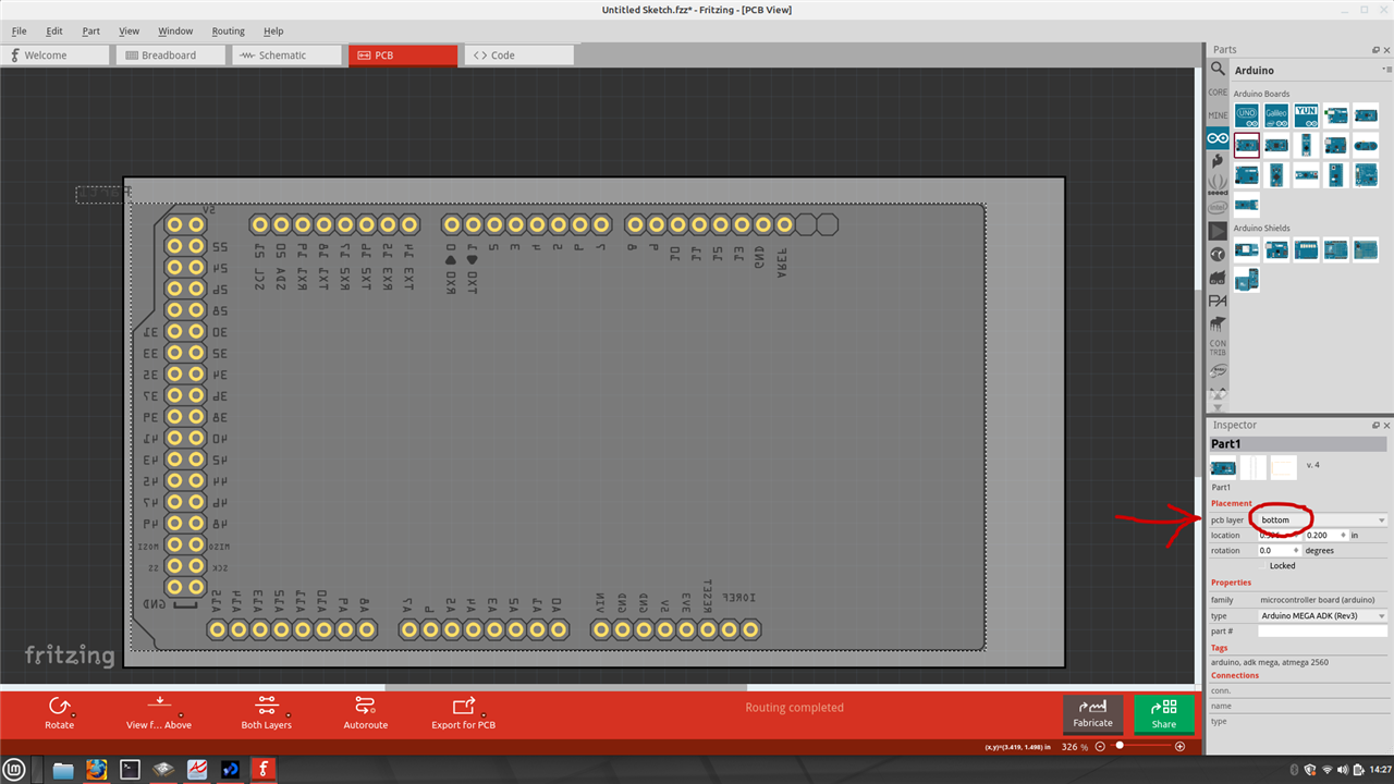
How do you mount a Mega on a PCB?

I'm using a Arduino Mega for a project and wanted to use Fritzing to create a PCB layout. The footprint for the Mega reflects the pinout of the motherboard. If I create a pin pattern on the board to mount the Mega directly to the board, then the pins need to be reversed. The Mega is flipped over and mounted face down on the PCB reversing the pinout.

I cannot find a pinout that reflects the Mega face down on a PCB. I would assume that is the way to install the board and not have a collection of jumpers running from the Mega board back to the PCB. If anyone has an insight I would welcome the input?

image

  • Sign in to reply
  • Cancel

Top Replies

  • Andrew J
    Andrew J over 3 years ago +2
    I assume the PCB is plated through-hole? Put the footprint on the reverse of the PCB but actually solder the MEGA (or headers) onto the front of the board. That would work wouldn’t it?
  • BigG
    BigG over 3 years ago in reply to colporteur +2
    I would change the background colour so that you can see the white font. I did a quick test to prove and it is quite straightforward. If this is what you need, then I can place the modified fritzing…
  • BigG
    BigG over 3 years ago +1
    In PCB mode, click on the footprint and then change "pcb layer" to bottom.
  • Andrew J
    0 Andrew J over 3 years ago

    I assume the PCB is plated through-hole?  Put the footprint on the reverse of the PCB but actually solder the MEGA (or headers) onto the front of the board.  That would work wouldn’t it?

    • Cancel
    • Vote Up +2 Vote Down
    • Sign in to reply
    • Verify Answer
    • Cancel
  • colporteur
    0 colporteur over 3 years ago in reply to Andrew J

    Thanks for the response. Your suggestion was my original thought. The Mega mounts on the backside of the PCB. Not a solution I have used before therefore it seemed strange. First time using a Mega in a project also.

    • Cancel
    • Vote Up 0 Vote Down
    • Sign in to reply
    • Verify Answer
    • Cancel
  • Andrew J
    0 Andrew J over 3 years ago in reply to colporteur

    Yes, that would work too!  Which side to solder the Mega too might get dictated by any encasement?  Specifically, how thick the case would be and access to the USB and Power ports once soldered; I was assuming you wanted to keep all parts on one side.

    • Cancel
    • Vote Up 0 Vote Down
    • Sign in to reply
    • Verify Answer
    • Cancel
  • colporteur
    0 colporteur over 3 years ago

    I stumbled on a work around to this question. The answer appears to the application. I took some screen shots of the Mega footprint while placing the component. I will attempt to explain my understanding.

    image

    The image far left is taken from Arduino webpage. The board has a few more pins than the Mega footprint in Fritzing but it will do for a visual representation of the Mega board.

    Image A is the Mega footprint found in Fritzing. The pin layout reflects the Arduino image shown. The image was imported while the View menu (second from left in red box), was set to View from Above.

    Image B is the Mega footprint with the View Menu was changed to View from Below.

    Both Image A and B are incorrect orientation for the Mega footprint. This is the reason I made this post.

    Image C is the Mega footprint imported while the View Menu is set to View from Below. If you were to look at a PCB from the below, the Mega would be on the other side of the PBB. This footprint orientation is correct. The pin asssignment labels would be correct if view from the bottom.

    Image D is the Mega footprint when View Menu is changed to View from Above. The orientation of the Mega is correct but the pin assignment labels are now incorrect.

    I plan to use Image C to layout a PCB. My plan is to send the board out to be made. I'm not confident the silk screening will be accurate.

    • Cancel
    • Vote Up 0 Vote Down
    • Sign in to reply
    • Verify Answer
    • Cancel
  • cstanton
    0 cstanton over 3 years ago

    Moved to Arduino group.

    • Cancel
    • Vote Up 0 Vote Down
    • Sign in to reply
    • Verify Answer
    • Cancel
  • BigG
    0 BigG over 3 years ago

    In PCB mode, click on the footprint and then change "pcb layer" to bottom.

    image

    • Cancel
    • Vote Up +1 Vote Down
    • Sign in to reply
    • Verify Answer
    • Cancel
  • colporteur
    0 colporteur over 3 years ago in reply to BigG

    Sorry for being tardy in my response. I've spent the last hour responding to messages regarding the successes I have had interacting with this site and let your message slip.

    Wait a minute? Your not standing at my desk. How would you know how long it has taken me to respond. I really have to get out more. This COVID isolation is making social media feel like human interaction. A little dig for cstanton:)

    Thank you for the share. I was not familiar with the selection option. Unfortunately, the silk screen number reversal thing, still happens, as I indicated in Image D above. I'm haven't mastered how to load additional footprints. Maybe the image errors are corrected in a more resent update.

    • Cancel
    • Vote Up 0 Vote Down
    • Sign in to reply
    • Verify Answer
    • Cancel
  • BigG
    0 BigG over 3 years ago in reply to colporteur
    colporteur said:
    Unfortunately, the silk screen number reversal thing, still happens, as I indicated in Image D above. 

    To resolve you would need to clone an Arduino Mega part and then modify that part (would need to use something like Inkscape) so that the silk screen is on the reverse.

    PS. The file you need to modify is called Arduino_ADK_MEGA_2560-Rev3_pcb.svg

    • Cancel
    • Vote Up 0 Vote Down
    • Sign in to reply
    • Verify Answer
    • Cancel
  • colporteur
    0 colporteur over 3 years ago in reply to BigG

    WOW, An answer I actually understand, with references I am familiar with and application tools I use. A trifecta 

    That deserves a Member in Good Standing badge for you!

    • Cancel
    • Vote Up +1 Vote Down
    • Sign in to reply
    • Verify Answer
    • Cancel
  • colporteur
    0 colporteur over 3 years ago in reply to BigG

    Never thought someone would do stuff with your suggestion?

    image

    I'm not seeing any silk screen. Do I have to change an option in Inkscape?

    • Cancel
    • Vote Up 0 Vote Down
    • Sign in to reply
    • Verify Answer
    • Cancel
>
element14 Community

element14 is the first online community specifically for engineers. Connect with your peers and get expert answers to your questions.

  • Members
  • Learn
  • Technologies
  • Challenges & Projects
  • Products
  • Store
  • About Us
  • Feedback & Support
  • FAQs
  • Terms of Use
  • Privacy Policy
  • Legal and Copyright Notices
  • Sitemap
  • Cookies

An Avnet Company © 2025 Premier Farnell Limited. All Rights Reserved.

Premier Farnell Ltd, registered in England and Wales (no 00876412), registered office: Farnell House, Forge Lane, Leeds LS12 2NE.

ICP 备案号 10220084.

Follow element14

  • X
  • Facebook
  • linkedin
  • YouTube