element14 Community
element14 Community
    Register Log In
  • Site
  • Search
  • Log In Register
  • About Us
  • Community Hub
    Community Hub
    • What's New on element14
    • Feedback and Support
    • Benefits of Membership
    • Personal Blogs
    • Members Area
    • Achievement Levels
  • Learn
    Learn
    • Ask an Expert
    • eBooks
    • element14 presents
    • Learning Center
    • Tech Spotlight
    • STEM Academy
    • Webinars, Training and Events
    • Learning Groups
  • Technologies
    Technologies
    • 3D Printing
    • FPGA
    • Industrial Automation
    • Internet of Things
    • Power & Energy
    • Sensors
    • Technology Groups
  • Challenges & Projects
    Challenges & Projects
    • Design Challenges
    • element14 presents Projects
    • Project14
    • Arduino Projects
    • Raspberry Pi Projects
    • Project Groups
  • Products
    Products
    • Arduino
    • Avnet Boards Community
    • Dev Tools
    • Manufacturers
    • Multicomp Pro
    • Product Groups
    • Raspberry Pi
    • RoadTests & Reviews
  • Store
    Store
    • Visit Your Store
    • Choose another store...
      • Europe
      •  Austria (German)
      •  Belgium (Dutch, French)
      •  Bulgaria (Bulgarian)
      •  Czech Republic (Czech)
      •  Denmark (Danish)
      •  Estonia (Estonian)
      •  Finland (Finnish)
      •  France (French)
      •  Germany (German)
      •  Hungary (Hungarian)
      •  Ireland
      •  Israel
      •  Italy (Italian)
      •  Latvia (Latvian)
      •  
      •  Lithuania (Lithuanian)
      •  Netherlands (Dutch)
      •  Norway (Norwegian)
      •  Poland (Polish)
      •  Portugal (Portuguese)
      •  Romania (Romanian)
      •  Russia (Russian)
      •  Slovakia (Slovak)
      •  Slovenia (Slovenian)
      •  Spain (Spanish)
      •  Sweden (Swedish)
      •  Switzerland(German, French)
      •  Turkey (Turkish)
      •  United Kingdom
      • Asia Pacific
      •  Australia
      •  China
      •  Hong Kong
      •  India
      •  Korea (Korean)
      •  Malaysia
      •  New Zealand
      •  Philippines
      •  Singapore
      •  Taiwan
      •  Thailand (Thai)
      • Americas
      •  Brazil (Portuguese)
      •  Canada
      •  Mexico (Spanish)
      •  United States
      Can't find the country/region you're looking for? Visit our export site or find a local distributor.
  • Translate
  • Profile
  • Settings
Dev Tools
  • Products
  • More
Dev Tools
Forum regarding mosfet configuration
  • Forum
  • Documents
  • Files
  • Members
  • Mentions
  • Sub-Groups
  • Tags
  • More
  • Cancel
  • New
Join Dev Tools to participate - click to join for free!
Actions
  • Share
  • More
  • Cancel
Forum Thread Details
  • Replies 3 replies
  • Subscribers 79 subscribers
  • Views 485 views
  • Users 0 members are here
Related

regarding mosfet configuration

msrinivasan19995
msrinivasan19995 over 8 years ago

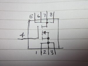
guys i'm going to use  two 40v mosfet in synchronous mode of operation for my buck converter. I have chosen SON package type. I have doubt regarding its structure. It has 4 drain, 3 source, 1 gate. Can we use two mosfet in the same  single package or 2 different packages are required. I can't understand why different modules various drains and source are available for single package.I 'm sharing the IC which i'm going to use. Suggestions are welcome.

CSD18512Q5B 40V N-Channel NexFETTm Power MOSFET | TI.com

  • Sign in to reply
  • Cancel

Top Replies

  • jc2048
    jc2048 over 8 years ago in reply to msrinivasan19995 +2
    Personally, I make symbols like this for the schematic, so I can see the pin numbers. But other people probably have other ways of doing it. In this case you've got the complication of the thermal pad…
  • jc2048
    jc2048 over 8 years ago +1
    I'm not quite sure I'm understanding your question properly. The device you link to is a single MOSFET. There are multiple package connections to the source and the drain. On a PCB you would connect all…
  • msrinivasan19995
    msrinivasan19995 over 8 years ago +1
    I'm new to this kind of packages. So i had doubt regarding various source pad and drain pad. I have worked basically on through hole mosfet's. So this kind of doubt araised. The device you link to is a…
  • jc2048
    jc2048 over 8 years ago

    I'm not quite sure I'm understanding your question properly.


    The device you link to is a single MOSFET. There are multiple package connections to the source and the drain. On a PCB you would connect all the drain pins together and all the source pins together. The reason for having multiple pins is that the current that the device can handle is so high it is too much for one pin and bond wire by itself [I'm impressed that they can manage 32A continuous with just three source pins, to be honest]. Even if you operate the device at a much lower current, still join the pins together - you'll only achieve the rDSon values in the datasheet if you use the device the way they intend [it won't make all that much difference, but why throw away something you are being given for free].


    If you want two MOSFETs in one package, they are available. Make sure that the package will be able to dissipate the heat of the two, though [you'll have to do all your thermal calculations again].

    • Cancel
    • Vote Up +1 Vote Down
    • Sign in to reply
    • Cancel
  • msrinivasan19995
    msrinivasan19995 over 8 years ago

    I'm new to this kind of packages. So i had doubt regarding various source pad and drain pad. I have worked basically on through hole mosfet's. So this kind of doubt araised.


    The device you link to is a single MOSFET. There are multiple package connections to the source and the drain. On a PCB you would connect all the drain pins together and all the source pins together.


    In the PCB design, can you elaborate how to connect all the drain's together and source together.


    with regards,

    Srinivasan

    • Cancel
    • Vote Up +1 Vote Down
    • Sign in to reply
    • Cancel
  • jc2048
    jc2048 over 8 years ago in reply to msrinivasan19995

    Personally, I make symbols like this for the schematic, so I can see the pin numbers. But other people probably have other ways of doing it. In this case you've got the complication of the thermal pad underneath and you've got to decide whether 5,6,7,8 and the thermal pad are all one, or whether they are all separate, or whether you put the thermal pad in by hand afterwards. The Eagle experts here should be able to guide you as to the best way to do it with that package. [You might need a new question in the Eagle area.]


    image


    Your tracks [source and drain] are going to be areas of copper at these sorts of current levels (I'm asssuming you haven't chosen a 30A MOSFET for switching an amp or two). So the source pins will all fall within the source copper area and the drain pins and heat pad will fall within the drain copper area. Do use a track for the gate, though, because you want to keep the capacitance down (the gate charge figure is high enough already without adding to the load for your controller chip).

    • Cancel
    • Vote Up +2 Vote Down
    • Sign in to reply
    • Cancel
element14 Community

element14 is the first online community specifically for engineers. Connect with your peers and get expert answers to your questions.

  • Members
  • Learn
  • Technologies
  • Challenges & Projects
  • Products
  • Store
  • About Us
  • Feedback & Support
  • FAQs
  • Terms of Use
  • Privacy Policy
  • Legal and Copyright Notices
  • Sitemap
  • Cookies

An Avnet Company © 2025 Premier Farnell Limited. All Rights Reserved.

Premier Farnell Ltd, registered in England and Wales (no 00876412), registered office: Farnell House, Forge Lane, Leeds LS12 2NE.

ICP 备案号 10220084.

Follow element14

  • X
  • Facebook
  • linkedin
  • YouTube