element14 Community
element14 Community
    Register Log In
  • Site
  • Search
  • Log In Register
  • Community Hub
    Community Hub
    • What's New on element14
    • Feedback and Support
    • Benefits of Membership
    • Personal Blogs
    • Members Area
    • Achievement Levels
  • Learn
    Learn
    • Ask an Expert
    • eBooks
    • element14 presents
    • Learning Center
    • Tech Spotlight
    • STEM Academy
    • Webinars, Training and Events
    • Learning Groups
  • Technologies
    Technologies
    • 3D Printing
    • FPGA
    • Industrial Automation
    • Internet of Things
    • Power & Energy
    • Sensors
    • Technology Groups
  • Challenges & Projects
    Challenges & Projects
    • Design Challenges
    • element14 presents Projects
    • Project14
    • Arduino Projects
    • Raspberry Pi Projects
    • Project Groups
  • Products
    Products
    • Arduino
    • Avnet Boards Community
    • Dev Tools
    • Manufacturers
    • Multicomp Pro
    • Product Groups
    • Raspberry Pi
    • RoadTests & Reviews
  • Store
    Store
    • Visit Your Store
    • Choose another store...
      • Europe
      •  Austria (German)
      •  Belgium (Dutch, French)
      •  Bulgaria (Bulgarian)
      •  Czech Republic (Czech)
      •  Denmark (Danish)
      •  Estonia (Estonian)
      •  Finland (Finnish)
      •  France (French)
      •  Germany (German)
      •  Hungary (Hungarian)
      •  Ireland
      •  Israel
      •  Italy (Italian)
      •  Latvia (Latvian)
      •  
      •  Lithuania (Lithuanian)
      •  Netherlands (Dutch)
      •  Norway (Norwegian)
      •  Poland (Polish)
      •  Portugal (Portuguese)
      •  Romania (Romanian)
      •  Russia (Russian)
      •  Slovakia (Slovak)
      •  Slovenia (Slovenian)
      •  Spain (Spanish)
      •  Sweden (Swedish)
      •  Switzerland(German, French)
      •  Turkey (Turkish)
      •  United Kingdom
      • Asia Pacific
      •  Australia
      •  China
      •  Hong Kong
      •  India
      •  Korea (Korean)
      •  Malaysia
      •  New Zealand
      •  Philippines
      •  Singapore
      •  Taiwan
      •  Thailand (Thai)
      • Americas
      •  Brazil (Portuguese)
      •  Canada
      •  Mexico (Spanish)
      •  United States
      Can't find the country/region you're looking for? Visit our export site or find a local distributor.
  • Translate
  • Profile
  • Settings
Autodesk EAGLE
  • Products
  • More
Autodesk EAGLE
EAGLE User Chat (English) 9v Battery - VDD and Ground Nets not connecting to battery
  • Blog
  • Forum
  • Documents
  • Events
  • Polls
  • Files
  • Members
  • Mentions
  • Sub-Groups
  • Tags
  • More
  • Cancel
  • New
Join Autodesk EAGLE to participate - click to join for free!
Actions
  • Share
  • More
  • Cancel
Forum Thread Details
  • State Not Answered
  • Replies 6 replies
  • Subscribers 171 subscribers
  • Views 1852 views
  • Users 0 members are here
Related

9v Battery - VDD and Ground Nets not connecting to battery

Former Member
Former Member over 10 years ago

As the subject describes, I am having trouble connecting my +VDD and -Ground nets to the 9v battery on my current board.


I am new to eagle software and am using some Sparkfun libraries. Can anybody provide any insight?


I have fully designed the schematic with great success. When switching to board view, to begin tracing out the components - I wanted to start with the source: a 9v battery (thank you sparkfun for the cradle footprint). I have the 9v going to a 5v regulator. The input of the regulator I have connected to the net labeled "VDD" and the output is connected to the net labeled "VCC."


The issue is that in schematic view, the battery's + and - terminals clearly are connected to the VDD and Ground nets going to the 5v regulator inputs. When switching to the board view, the battery's terminals will not accept placing a trace to connect to the regulators footprint.


What am I doing wrong? The cradle has 2 pins providing a direct connection to the board from the battery. The footprint for these pins, or the two pads, will not accept a trace being placed to make the connection to the regulator.


Can anybody identify where my mistake lies?

imageimage

  • Sign in to reply
  • Cancel
  • autodeskguest
    0 autodeskguest over 10 years ago

    Matt Horner wrote:


    As the subject describes, I am having trouble connecting my +VDD and

    -Ground nets to the 9v battery on my current board.


    I am new to eagle software and am using some Sparkfun libraries. Can

    anybody provide any insight?


    I have fully designed the schematic with great success. When switching

    to board view, to begin tracing out the components - I wanted to start

    with the source: a 9v battery (thank you sparkfun for the cradle

    footprint). I have the 9v going to a 5v regulator. The input of the

    regulator I have connected to the net labeled "VDD" and the output is

    connected to the net labeled "VCC."


    The issue is that in schematic view, the battery's + and - terminals

    clearly are connected to the VDD and Ground nets going to the 5v

    regulator inputs. When switching to the board view, the battery's

    terminals will not accept placing a trace to connect to the regulators

    footprint.


    What am I doing wrong? The cradle has 2 pins providing a direct

    connection to the board from the battery. The footprint for these pins,

    or the two pads, will not accept a trace being placed to make the

    connection to the regulator.


    Can anybody identify where my mistake lies?


    I think you (mis-)used the bus command to draw part of your

    connections.

    That won't work. The purpose of a bus is to bundle multiply signals.

    It never connects directly to a pin. A netstub is allways needed to

    determine which signal (from the bus) is connected to the pin.

    --


    Lorenz


    • Cancel
    • Vote Up 0 Vote Down
    • Sign in to reply
    • Verify Answer
    • Cancel
  • autodeskguest
    0 autodeskguest over 10 years ago

    Run ERC and you will get a list of issues you need to fix.


    • Cancel
    • Vote Up 0 Vote Down
    • Sign in to reply
    • Verify Answer
    • Cancel
  • dougw
    0 dougw over 10 years ago

    It looks like the connections are not properly made on your schematic.

    The blue traces on the schematic are not proper connections they are probably bus lines or just blue lines.

    To make these connections, use the Wire tool on the green 91 Nets layer.

    image

    • Cancel
    • Vote Up 0 Vote Down
    • Sign in to reply
    • Verify Answer
    • Cancel
  • autodeskguest
    0 autodeskguest over 10 years ago in reply to dougw

    On 01/11/14 05:56, Douglas Wong wrote:

    To make these connections, use the Wire tool on the green 91 Nets layer.


    NO! BAD ADVICE!


    Don't use the "WIRE" tool to make nets, use the "NET" tool.


    (Although the wire tool is closer to working than the bus tool!)


    • Cancel
    • Vote Up 0 Vote Down
    • Sign in to reply
    • Verify Answer
    • Cancel
  • ingit
    0 ingit over 10 years ago

    Not to worry much about it follow these simple steps image image

    1.) Open the layer selection dialog box.

    image

    2.) In that select the "Pins Layer" and hit apply.

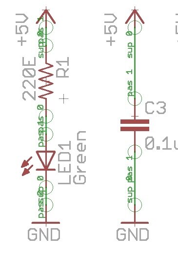
    3.) After that you will see some bubble kind of things around the pins of each component, as shown below.

    image

    4.) Now connect a net to that bubble and connect to another components pin with the bubble, or simply use the junction tool, below buss tool.

    Actually connection is from bubble to bubble, not any other part of the component.

    Connection is possible when there is a bubble. If pins layer is disabled then also connection is between bubbles.

    image

    that plus symbol with a dot in center. use that.

    If there is no connection between two pins i.e. bubbles, no net will be seen on the board.image image

    • Cancel
    • Vote Up 0 Vote Down
    • Sign in to reply
    • Verify Answer
    • Cancel
element14 Community

element14 is the first online community specifically for engineers. Connect with your peers and get expert answers to your questions.

  • Members
  • Learn
  • Technologies
  • Challenges & Projects
  • Products
  • Store
  • About Us
  • Feedback & Support
  • FAQs
  • Terms of Use
  • Privacy Policy
  • Legal and Copyright Notices
  • Sitemap
  • Cookies

An Avnet Company © 2025 Premier Farnell Limited. All Rights Reserved.

Premier Farnell Ltd, registered in England and Wales (no 00876412), registered office: Farnell House, Forge Lane, Leeds LS12 2NE.

ICP 备案号 10220084.

Follow element14

  • X
  • Facebook
  • linkedin
  • YouTube